|
|
|
PDF ADL5602 Data sheet ( Hoja de datos )
| Número de pieza | ADL5602 | |
| Descripción | 50 MHz To 4.0 GHz RF/IF Gain Block | |
| Fabricantes | Analog Devices | |
| Logotipo | ||
Hay una vista previa y un enlace de descarga de ADL5602 (archivo pdf) en la parte inferior de esta página. Total 16 Páginas | ||
|
No Preview Available !
www.DataSheet4U.com
FEATURES
Fixed gain of 20 dB
Operation from 50 MHz to 4.0 GHz
Highest dynamic range gain block
Input/output internally matched to 50 Ω
Integrated bias control circuit
OIP3 of 42.0 dBm at 2.0 GHz
P1dB of 19.3 dBm at 2.0 GHz
Noise figure of 3.3 dB at 2.0 GHz
Single 5 V power supply
Low quiescent current of 89 mA
Thermally efficient SOT-89 package
ESD rating of ±1.5 kV (Class 1C)
GENERAL DESCRIPTION
The ADL5602 is a broadband 20 dB linear amplifier that operates
at frequencies up to 4 GHz. The device can be used in a wide
variety of cellular, CATV, military, and instrumentation equipment.
The ADL5602 provides the highest dynamic range available
from an internally matched gain block. This is accomplished
by providing extremely low noise figures and very high OIP3
specifications simultaneously, across the entire 4 GHz
frequency range.
The ADL5602 provides a gain of 20 dB, which is stable over
frequency, temperature, power supply, and from device to
device. The device is internally matched to 50 Ω at the input
and output, making the ADL5602 very easy to implement in a
wide variety of applications. Only input/output ac coupling
capacitors, power supply decoupling capacitors, and an external
inductor are required for operation.
50 MHz to 4.0 GHz
RF/IF Gain Block
ADL5602
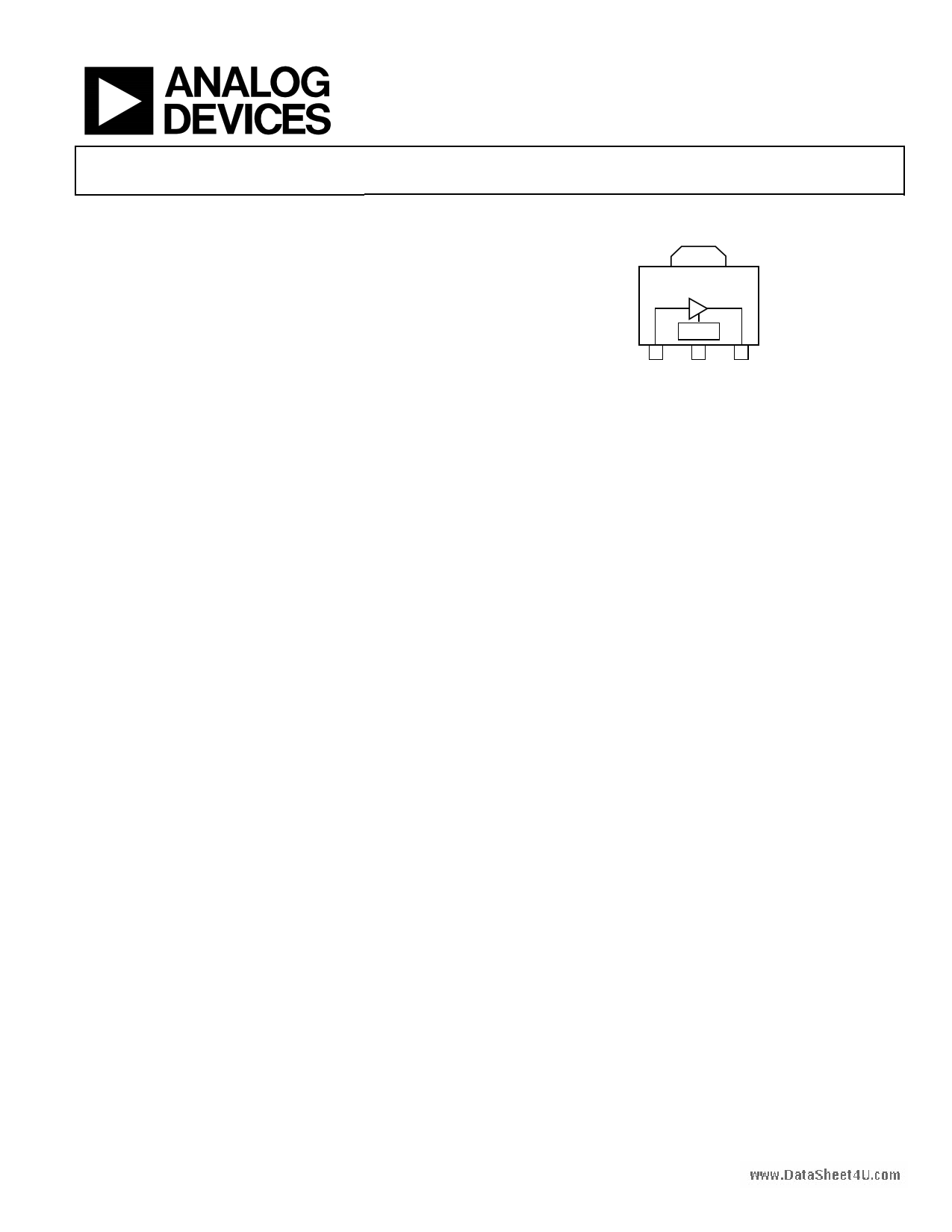
FUNCTIONAL BLOCK DIAGRAM
GND
(2)
ADL5602
1
RFIN
BIAS
23
GND RFOUT
Figure 1.
The ADL5602 is fabricated on an InGaP HBT process and has
an ESD rating of ±1.5 kV (Class 1C). The device is available in a
thermally efficient SOT-89 package.
The ADL5602 consumes 89 mA on a single 5 V supply and is
fully specified for operation from −40°C to +85°C.
A fully populated RoHS-compliant evaluation board is available.
Rev. 0
Information furnished by Analog Devices is believed to be accurate and reliable. However, no
responsibility is assumed by Analog Devices for its use, nor for any infringements of patents or other
rights of third parties that may result from its use. Specifications subject to change without notice. No
license is granted by implication or otherwise under any patent or patent rights of Analog Devices.
Trademarksandregisteredtrademarksarethepropertyoftheirrespectiveowners.
One Technology Way, P.O. Box 9106, Norwood, MA 02062-9106, U.S.A.
Tel: 781.329.4700
www.analog.com
Fax: 781.461.3113
©2009 Analog Devices, Inc. All rights reserved.
1 page 
www.DataSheet4U.com
Parameter
POWER INTERFACE
Supply Voltage (VCC)
Supply Current
vs. Temperature
Power Dissipation
Conditions
VCC
−40°C ≤ TA ≤ +85°C
VCC = 5 V
ADL5602
Min Typ
4.5 5
89
±3
0.45
Max Unit
5.5 V
106 mA
mA
W
TYPICAL SCATTERING PARAMETERS (S PARAMETERS)
VCC = 5 V and TA = 25°C, the effects of the test fixture have been de-embedded up to the pins of the device.
Table 2.
Frequency
(MHz)
50
100
150
200
250
300
350
400
450
500
550
600
650
700
750
800
850
900
950
1000
1050
1100
1150
1200
1250
1300
1350
1400
1450
1500
1550
1600
1650
1700
1750
1800
1850
1900
1950
S11
Magnitude (dB)
−12.75
−8.98
−10.11
−11.97
−13.85
−15.69
−17.40
−19.17
−20.86
−22.52
−24.32
−26.07
−27.89
−30.79
−34.53
−42.59
−46.49
−34.26
−29.55
−25.87
−23.03
−21.25
−19.31
−17.72
−16.13
−14.81
−13.65
−12.68
−11.72
−10.92
−10.21
−9.58
−9.05
−8.52
−8.13
−7.76
−7.46
−7.19
−6.98
Angle (°)
+32.81
−7.00
−34.04
−50.46
−62.42
−72.90
−81.30
−88.48
−97.45
−107.32
−112.89
−120.03
−128.79
−133.19
−136.03
−130.76
−2.93
+15.99
+9.83
+5.52
+1.85
+0.10
−1.89
−4.09
−6.53
−8.71
−10.01
−11.33
−12.65
−13.56
−14.37
−15.37
−15.74
−16.73
−17.13
−17.59
−17.76
−17.92
−17.84
S21
Magnitude (dB)
18.14
15.77
17.27
18.50
19.21
19.64
19.90
20.07
20.18
20.25
20.32
20.35
20.39
20.42
20.42
20.46
20.47
20.47
20.48
20.48
20.47
20.45
20.45
20.40
20.35
20.31
20.24
20.18
20.11
20.04
19.97
19.88
19.80
19.72
19.64
19.57
19.50
19.43
19.39
Angle (°)
+163.00
−179.92
−169.01
−168.73
−171.01
−173.77
−176.45
−178.86
+178.79
+176.86
+174.84
+173.09
+171.35
+169.67
+167.93
+166.48
+164.85
+163.17
+161.77
+160.25
+158.65
+157.18
+155.50
+153.93
+152.44
+150.88
+149.35
+147.91
+146.40
+145.13
+143.86
+142.58
+141.40
+140.23
+139.13
+138.12
+137.16
+136.25
+135.31
S12
Magnitude (dB)
−25.27
−27.59
−26.11
−24.84
−24.14
−23.70
−23.43
−23.26
−23.14
−23.08
−23.00
−22.97
−22.93
−22.91
−22.91
−22.88
−22.88
−22.86
−22.86
−22.86
−22.89
−22.90
−22.92
−22.96
−23.04
−23.07
−23.16
−23.22
−23.32
−23.39
−23.49
−23.57
−23.69
−23.76
−23.87
−23.94
−24.05
−24.13
−24.18
Angle (°)
−9.54
+4.56
+16.05
+16.55
+14.79
+12.89
+11.02
+9.65
+8.07
+7.11
+6.15
+5.24
+4.35
+3.72
+2.93
+2.30
+1.67
+0.98
+0.39
−0.21
−0.84
−1.43
−2.06
−2.72
−3.38
−4.04
−4.60
−5.06
−5.76
−6.16
−6.54
−6.93
−7.16
−7.45
−7.60
−7.80
−7.88
−7.91
−7.94
S22
Magnitude (dB)
−8.96
−7.07
−7.89
−9.33
−10.87
−12.23
−13.56
−14.79
−15.99
−17.02
−18.21
−19.45
−20.73
−22.22
−23.91
−26.35
−29.40
−34.27
−40.86
−31.44
−26.19
−23.27
−20.70
−18.67
−16.92
−15.44
−14.14
−13.12
−12.04
−11.20
−10.49
−9.77
−9.21
−8.66
−8.26
−7.91
−7.56
−7.35
−7.13
Angle (°)
−145.86
−178.96
+159.89
+147.22
+140.02
+136.16
+134.03
+132.79
+132.72
+133.33
+133.04
+135.06
+136.29
+136.96
+135.39
+136.07
+132.08
+116.48
+41.72
−10.36
−18.99
−22.34
−22.26
−24.44
−24.75
−25.79
−25.36
−25.73
−25.59
−25.40
−25.60
−25.59
−25.31
−25.42
−25.32
−24.96
−24.77
−24.46
−23.92
Rev. 0 | Page 5 of 16
5 Page 
www.DataSheet4U.com
BASIC CONNECTIONS
The basic connections for operating the ADL5602 are shown in
Figure 15. Recommended components are listed in Table 5. The
input and output should be ac-coupled with appropriately sized
capacitors (device characterization was performed with 0.1 μF
capacitors). A 5 V dc bias is supplied to the amplifier through
the bias inductor connected to RFOUT (Pin 3). The bias voltage
should be decoupled using a 1 μF capacitor, a 1.2 nF capacitor,
and a 68 pF capacitor.
GND VCC
C6
1µF
C5
(2) 1.2nF
C4
RFIN C1
0.1µF
ADL5602
123
68pF
L1
470nH
C2 RFOUT
0.1µF
Figure 15. Basic Connections
ADL5602
SOLDERING INFORMATION AND RECOMMENDED
PCB LAND PATTERN
Figure 16 shows the recommended land pattern for the ADL5602.
To minimize thermal impedance, the exposed paddle on the
package underside should be soldered down to a ground plane
along with Pin 2. If multiple ground layers exist, they should be
stitched together using vias. For more information on land
pattern design and layout, refer to AN-772 Application Note, A
Design and Manufacturing Guide for the Lead Frame Chip Scale
Package (LFCSP).
1.80mm
5.56mm 0.20mm
3.48mm
0.86mm
0.62mm
1.27mm
1.50mm
3.00mm
Figure 16. Recommended Land Pattern
Table 5. Recommended Components for Basic Connections
Frequency (MHz)
C1
C2
L1
50 to 4000
0.1 μF
0.1 μF
470 nH (Coilcraft 0603LS-NX or equivalent)
C4
68 pF
C5
1.2 nF
C6
1 μF
Rev. 0 | Page 11 of 16
11 Page | ||
| Páginas | Total 16 Páginas | |
| PDF Descargar | [ Datasheet ADL5602.PDF ] | |
Hoja de datos destacado
| Número de pieza | Descripción | Fabricantes |
| ADL5601 | 50 MHz to 4.0 GHz RF/IF Gain Block | Analog Devices |
| ADL5602 | 50 MHz To 4.0 GHz RF/IF Gain Block | Analog Devices |
| ADL5604 | 700 MHz To 2700 MHz 1 W RF Driver Amplifier | Analog Devices |
| ADL5605 | 1W RF Driver Amplifier | Analog Devices |
| Número de pieza | Descripción | Fabricantes |
| SLA6805M | High Voltage 3 phase Motor Driver IC. |
Sanken |
| SDC1742 | 12- and 14-Bit Hybrid Synchro / Resolver-to-Digital Converters. |
Analog Devices |
|
DataSheet.es es una pagina web que funciona como un repositorio de manuales o hoja de datos de muchos de los productos más populares, |
| DataSheet.es | 2020 | Privacy Policy | Contacto | Buscar |