|
|
|
PDF ADN4662 Data sheet ( Hoja de datos )
| Número de pieza | ADN4662 | |
| Descripción | LVDS Differential Line Receiver | |
| Fabricantes | Analog Devices | |
| Logotipo | ||
Hay una vista previa y un enlace de descarga de ADN4662 (archivo pdf) en la parte inferior de esta página. Total 12 Páginas | ||
|
No Preview Available !
www.DataSheet4U.com
FEATURES
±15 kV ESD protection on input pins
400 Mbps (200 MHz) switching rates
Flow-through pinout simplifies PCB layout
2.5 ns maximum propagation delay
3.3 V power supply
High impedance outputs on power-down
Low power design: typically 3 mW (quiescent)
Interoperable with existing 5 V LVDS drivers
Accepts small swing (310 mV typical) differential signal
levels
Supports open, short, and terminated input fail-safe
0 V to −100 mV threshold region
Conforms to TIA/EIA-644 LVDS standard
Industrial operating temperature range: −40°C to +85°C
Available in surface-mount (SOIC) package
APPLICATIONS
Point-to-point data transmission
Multidrop buses
Clock distribution networks
Backplane receivers
GENERAL DESCRIPTION
The ADN4662 is a single, CMOS, low voltage differential
signaling (LVDS) line receiver offering data rates of over
400 Mbps (200 MHz), and ultralow power consumption.
It features a flow-through pinout for easy PCB layout and
separation of input and output signals.
The device accepts low voltage (310 mV typical) differential
input signals and converts them to a single-ended 3 V TTL/
CMOS logic level.
Single, 3 V, CMOS, LVDS
Differential Line Receiver
ADN4662
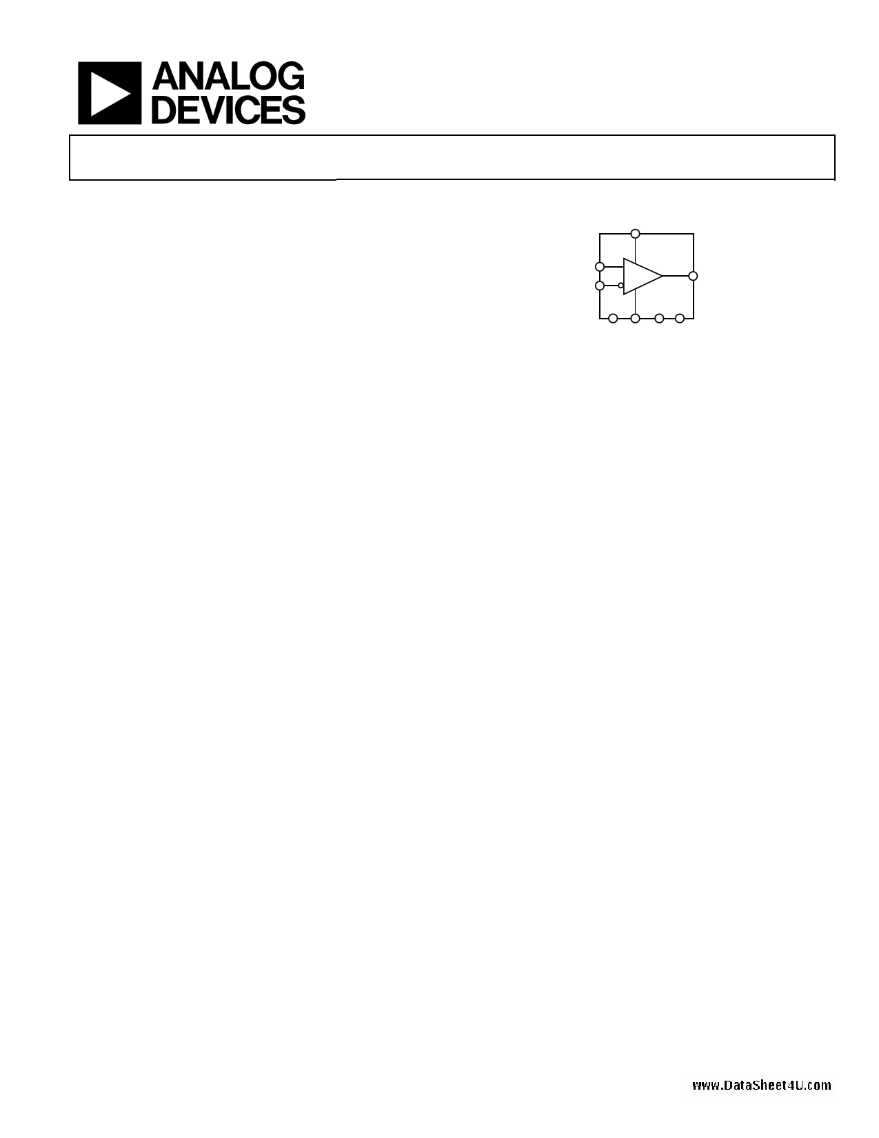
FUNCTIONAL BLOCK DIAGRAM
VCC
ADN4662
RIN+
RIN–
ROUT
NC GND NC NC
Figure 1.
The ADN4662 and its companion driver, the ADN4661, offer a
new solution to high speed, point-to-point data transmission,
and a low power alternative to emitter-coupled logic (ECL) or
positive emitter-coupled logic (PECL).
Rev. 0
Information furnished by Analog Devices is believed to be accurate and reliable. However, no
responsibility is assumed by Analog Devices for its use, nor for any infringements of patents or other
rights of third parties that may result from its use. Specifications subject to change without notice. No
license is granted by implication or otherwise under any patent or patent rights of Analog Devices.
Trademarksandregisteredtrademarksarethepropertyoftheirrespectiveowners.
One Technology Way, P.O. Box 9106, Norwood, MA 02062-9106, U.S.A.
Tel: 781.329.4700
www.analog.com
Fax: 781.461.3113
©2009 Analog Devices, Inc. All rights reserved.
1 page 
www.DataSheet4U.com
Test Circuits and Timing Diagrams
SIGNAL
GENERATOR
VCC
50Ω
RIN+
RIN–
50Ω
ROUT
CL
CL = LOAD AND TEST JIG CAPACITANCE
Figure 2. Test Circuit for Receiver Propagation Delay and Transition Time
RIN–
RIN+
0V (DIFFERENTIAL)
tPLHD
VID = 200mV
1.2V
tPHLD
80% 80%
1.3V
1.1V
VOH
ROUT
1.5V
1.5V
20%
20%
tTLH
tTHL
VOL
Figure 3. Receiver Propagation Delay and Transition Time Waveforms
ADN4662
Rev. 0 | Page 5 of 12
5 Page 
www.DataSheet4U.com
THEORY OF OPERATION
The ADN4662 is a single line receiver for low voltage
differential signaling. It takes a differential input signal of
310 mV typically and converts it into a single-ended 3 V
TTL/CMOS logic signal.
A differential current input signal, received via a transmission
medium, such as a twisted pair cable, develops a voltage across
a terminating resistor, RT. This resistor is chosen to match the
characteristic impedance of the medium, typically around
100 Ω. The differential voltage is detected by the receiver and
converted back into a single-ended logic signal.
When the noninverting receiver input, RIN+, is positive with
respect to the inverting input RIN− (current flows through RT
from RIN+ to RIN−), then ROUT is high. When the noninverting
receiver input RIN+ is negative with respect to the inverting
input RIN− (current flows through RT from RIN− to RIN+), then
ROUT is low.
The ADN4662 differential line receiver is capable of receiving
signals of 100 mV over a ±1 V common-mode range centered
around 1.2 V. This relates to the typical driver offset voltage
value of 1.2 V. The signal originating from the driver is centered
around 1.2 V and may shift ±1 V around this center point. This
±1 V shifting may be caused by a difference in the ground
potential of the driver and receiver, the common-mode effect of
coupled noise, or both.
Using the ADN4663 as a driver, the received differential current
is between 2.5 mA and 4.5 mA (typically 3.1 mA), developing
between 250 mV and 450 mV across a 100 Ω termination resis-
tor. The received voltage is centered around the receiver offset of
1.2 V. In other words, the noninverting receiver input is typically
ADN4662
(1.2 V + [310 mV/2]) = 1.355 V, and the inverting receiver input
(1.2 V − [310 mV/2]) = 1.045 V for Logic 1. For Logic 0, the
inverting and noninverting input voltages are reversed. Note that
because the differential voltage reverses polarity, the peak-to-peak
voltage swing across RT is twice the differential voltage.
Current mode signalling offers considerable advantages over
voltage mode signalling, such as RS-422. The operating current
remains fairly constant with increased switching frequency,
whereas with voltage mode drivers the current increases
exponentially in most cases. This is caused by the overlap as
internal gates switch between high and low, which causes currents
to flow from VCC to ground. A current mode device simply reverses
a constant current between its two outputs, with no significant
overlap currents.
This is similar to emitter-coupled logic (ECL) and positive emitter-
coupled logic (PECL), but without the high quiescent current of
ECL and PECL.
APPLICATIONS INFORMATION
Figure 23 shows a typical application for point-to-point data
transmission using the ADN4663 as the driver.
0.1µF
VCC
3.3V
+ 10µF
TANTALUM
0.1µF
VCC
3.3V
+ 10µF
TANTALUM
ADN4661
DOUT+
RIN+
ADN4662
DIN
RT 100Ω
DOUT–
RIN–
ROUT
GND
GND
Figure 23. Typical Application Circuit
Rev. 0 | Page 11 of 12
11 Page | ||
| Páginas | Total 12 Páginas | |
| PDF Descargar | [ Datasheet ADN4662.PDF ] | |
Hoja de datos destacado
| Número de pieza | Descripción | Fabricantes |
| ADN4661 | High Speed Differential Driver | Analog Devices |
| ADN4662 | LVDS Differential Line Receiver | Analog Devices |
| ADN4663 | Dual 3V CMOS LVDS High Speed Differential Driver | ANALOG DEVICES |
| ADN4663 | LVDS High Speed Differential Driver | Analog Devices |
| Número de pieza | Descripción | Fabricantes |
| SLA6805M | High Voltage 3 phase Motor Driver IC. |
Sanken |
| SDC1742 | 12- and 14-Bit Hybrid Synchro / Resolver-to-Digital Converters. |
Analog Devices |
|
DataSheet.es es una pagina web que funciona como un repositorio de manuales o hoja de datos de muchos de los productos más populares, |
| DataSheet.es | 2020 | Privacy Policy | Contacto | Buscar |