|
|
|
PDF ADIS16209 Data sheet ( Hoja de datos )
| Número de pieza | ADIS16209 | |
| Descripción | Dual-Axis Digital Inclinometer and Accelerometer | |
| Fabricantes | Analog Devices | |
| Logotipo | ||
Hay una vista previa y un enlace de descarga de ADIS16209 (archivo pdf) en la parte inferior de esta página. Total 16 Páginas | ||
|
No Preview Available !
Preliminary Technical Data
High-Accuracy, Dual-Axis
Digital Inclinometer and Accelerometer
ADIS16209
www.daFtaEsAhTeeUt4RuE.cSom
Dual-mode inclinometer system
Dual–axis, inclinometer configuration, ±30°
Single-axis, vertical operation, ±180°
High accuracy, 0.1°
14-bit digital inclination data, 0.025° resolution
14-bit digital acceleration data, 0.244 mg resolution
±1.7 g accelerometer measurement range
12-bit digital temperature sensor output
Digitally controlled sensitivity and bias calibration
Digitally controlled sample rate
Digitally controlled frequency response
Dual alarm settings with rate/threshold limits
Auxiliary digital I/O
Digitally activated self test
Digitally activated low power mode
SPI-compatible serial interfaceAuxiliary 12-bit ADC input
and DAC output
Single-supply operation: +3.0 V to +3.6 V
3500 g powered shock survivability
APPLICATIONS
Platform control, stabilization, and alignment
Tilt sensing, inclinometers, leveling
Motion/position measurement
Monitor/alarm devices (security, medical, safety)
Navigation
GENERAL DESCRIPTION
The ADIS16209 is a high-accuracy, digital inclinometer, that
accommodates both single axis (±180°) and dual-axis (±30°)
operation. The standard supply voltage (+3.3 V) and SPI® serial
interface enable simple integration into most industrial system
designs. A simple internal register structure handles all output
data and configuration features. This includes access to the
following output data:
• Calibrated acceleration
• Accurate incline angles
• Power supply
• Internal temperature
• Auxiliary analog and digital input signals
• Diagnostic error flags
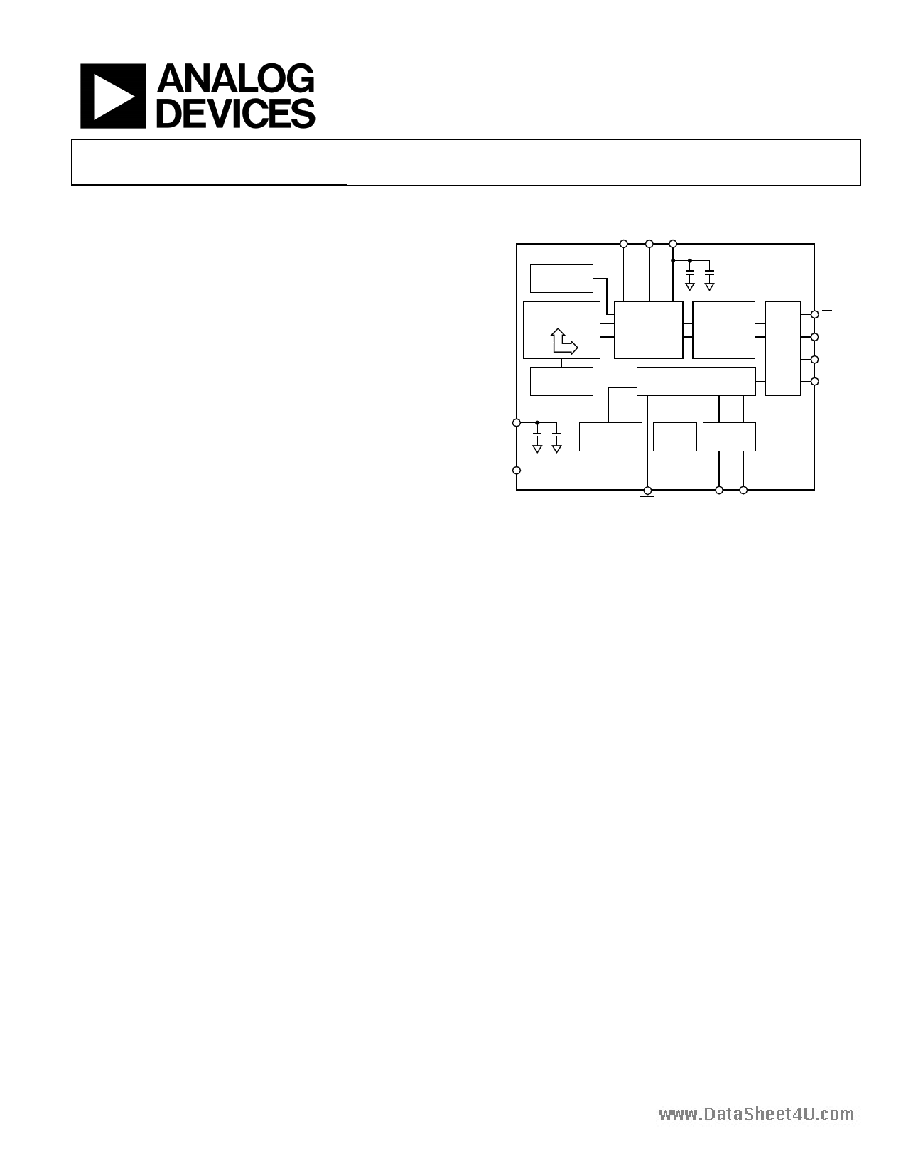
FUNCTIONAL BLOCK DIAGRAM
AUX AUX
ADC DAC VREF
ADIS16209
TEMPERATURE
SENSOR
DUAL-AXIS
ACCELEROMETER
SELF-TEST
SIGNAL
CONDITIONING
AND
CONVERSION
CALIBRATION
AND
DIGITAL
PROCESSING
DIGITAL
CONTROL
SPI
PORT
CS
SCLK
DIN
DOUT
VDD
GND
POWER
MANAGEMENT
ALARMS
AUXILIARY
I/O
RST
Figure 1.
DIO1 DIO2
• Programmable alarm conditions
Configurable operating parameters include
• Sample rate
• Power management
• Digital filtering
• Auxiliary analog and digital output
• Offset/null adjustment
• Self-test, for sensor’s mechanical structure
The ADIS16209 is available in a 9.2 mm × 9.2 mm × 3.9mm
LGA package that operates over a temperature range of −40°C
to +125°C. It is capable of being attached using standard RoHS-
compliant solder reflow processes.
Rev. PrA
Information furnished by Analog Devices is believed to be accurate and reliable. However, no
responsibility is assumed by Analog Devices for its use, nor for any infringements of patents or other
rights of third parties that may result from its use. Specifications subject to change without notice. No
license is granted by implication or otherwise under any patent or patent rights of Analog Devices.
Trademarksandregisteredtrademarksarethepropertyoftheirrespectiveowners.
One Technology Way, P.O. Box 9106, Norwood, MA 02062-9106, U.S.A.
Tel: 781.329.4700
www.analog.com
Fax: 781.461.3113
©2007 Analog Devices, Inc. All rights reserved.
1 page 
Preliminary Technical Data
ADIS16209
TIMING SPECIFICATIONS
TA = 25°C, VDD = 3.3 V, tilt = 0°, unless otherwise noted.
Table 2.
Parameter
www.dafStCaLsKheet4u.com
tDATARATE
tDATARATE
tCS
tDAV
tDSU
tDHD
tDF
tDR
tSFS
Description
Fast mode, SMPL_PRD ≤ 0x07 (fs ≥ 1024 Hz)
Normal mode, SMPL_PRD ≥ 0x08 (fs ≤ 910 Hz)
Chip select period, fast mode, SMPL_PRD ≤ 0x07 (fs ≥ 1024 Hz)
Chip select period, normal mode, SMPL_PRD ≥ 0x08 (fs ≤ 910 Hz)
Chip select to clock edge
Data output valid after SCLK edge
Data input setup time before SCLK rising edge
Data input hold time after SCLK rising edge
Data output fall time
Data output rise time
CS high after SCLK edge
1 Guaranteed by design, not tested.
Min1
0.01
0.01
40
100
48.8
24.4
48.8
5
Typ Max Unit
2.5 MHz
1.0 MHz
μs
μs
ns
100 ns
ns
ns
5 12.5 ns
5 12.5 ns
ns
TIMING DIAGRAMS
CS
SCLK
tDATARATE
tSTALL
tSTALL = tDATA RATE – 16/fSCLK
Figure 2. SPI Chip Select Timing
CS
SCLK
DOUT
DIN
tCS
1
MSB
W/R
23 4 5 6
tDAV
DB14
tDSU
DB13
DB12
tDHD
DB11
DB10
A5 A4 A3 A2
15 16
tSFS
DB2
DB1
LSB
D2 D1 LSB
Figure 3. SPI Timing
(Utilizing SPI Settings Typically Identified as Phase = 1, Polarity = 1)
CS
SCLK
DIN W/R
DATA FRAME
A5 A4 A3 A2 A1 A0 DC7 DC6 DC5 DC4 DC3 DC2 DC1 DC0
WRITE = 1
READ = 0
REGISTER ADDRESS
DATA FOR WRITE COMMANDS
DON’T CARE FOR READ COMMANDS
Figure 4. DIN Bit Sequence
Rev. PrA | Page 5 of 16
5 Page 
Preliminary Technical Data
ADIS16209
BASIC OPERATION
The ADIS16209 requires only power/ground and SPI
connections. The SPI is simple to hook up and is supported by
many common digital hardware platforms. Figure 21 provides a
www.dastiamspheleeht4ouo.cko-mup diagram, while Table 2, Figure 2, Figure 3
provide timing and bit assignments. Figure 4 provides the bit
sequence for accessing the register memory structure. Each
function within the ADIS16209 has its own register, which has a
unique, 6-bit address. Note that all 16 SCLK cycles are required
for the DIN bit sequence to configure the output for the next
data frame. The ADIS16209 supports full duplex mode
operation. Table 6 provides the entire user register map for the
ADIS16209. For each register, the lower byte’s address is given.
For those registers that have two bytes, the upper byte’s address
is simply the lower byte’s address, incremented by 0x01.
ADIS16209
CS
SCLK
DIN
DOUT
EMBEDDED
PROCESSOR/
DSP/FPGA
PF
SCK
MOSI
MISO
Figure 21. Typical SPI Hook-up
Many of the configuration registers have also been assigned
mirror locations in the flash memory, which effectively provides
them with a backup storage function. To assure the backup of
these registers, the COMMAND register provides an initiation
bit for manual flash updates. The ENDURANCE register
provides a running count of these events.
Table 6. User Register Map
Name
R/W Flash Backup
ENDURANCE R
Yes
SUPPLY_OUT R
No
XACCL_OUT R
No
YACCL_OUT R
No
AUX_ADC
R No
TEMP_OUT R
No
XINCL_OUT R
No
YINCL_OUT R
No
ROT_OUT
R No
XACCL_NULL R/W Yes
YACCL_NULL R/W Yes
XINCL_NULL R/W Yes
YINCL_NULL R/W Yes
ROT_NULL
R/W Yes
ALM_MAG1
ALM_MAG2
ALM_SMPL1
ALM_SMPL2
ALM_CTRL
AUX_DAC
GPIO_CTRL
MSC_CTRL
SMPL_PRD
AVG_CNT
SLP_CNT
STATUS
COMMAND
R/W Yes
R/W Yes
R/W Yes
R/W Yes
R/W Yes
No
R/W No
R/W No
R/W No
R/W Yes
R/W Yes
W Yes
R No
W No
Address
0x00
0x02
0x04
0x06
0x08
0x0A
0x0C
0x0E
0x10
0x12
0x14
0x16
0x18
0x1A
0x1C to 0x1F
0x20
0x22
0x24
0x26
0x28
0x2A to 0x2F
0x30
0x32
0x34
0x36
0x38
0x3A
0x3C
0x3E
Size (Bytes)
2
2
2
2
2
2
2
2
2
2
2
2
2
2
4
2
2
2
2
2
6
2
2
2
2
2
2
2
2
Function
Diagnostics, flash write counter (16-bit binary)
Output, power supply
Output, X-axis acceleration
Output, Y-axis acceleration
Output, auxiliary ADC
Output, temperature
Output, ±90° X-axis inclination
Output, ±90° Y-axis inclination
Output, ±180° vertical rotational position
Calibration, X-Axis acceleration offset null
Calibration, Y-axis acceleration offset null
Calibration, X-axis inclination offset null
Calibration, Y-axis inclination offset null
Calibration, vertical rotation offset null
Reserved, do not write to these locations
Alarm 1, amplitude threshold
Alarm 2, amplitude threshold
Alarm 1, sample period
Alarm 2, sample period
Alarm, source control register
Reserved
Auxiliary DAC data
Operation, digital I/O configuration and data
Operation, data-ready and self-test control
Operation, sample rate configuration
Operation, filter configuration
Operation, sleep mode control
Diagnostics, system status register
Operation, system command register
Reference
Table 7
Table 7
Table 7
Table 7
Table 7
Table 7
Table 7
Table 7
Table 16
Table 16
Table 17
Table 17
Table 17
Table 18
Table 18
Table 19
Table 19
Table 20
Table 14
Table 13
Table 12
Table 8
Table 10
Table 9
Table 21
Table 15
Rev. PrA | Page 11 of 16
11 Page | ||
| Páginas | Total 16 Páginas | |
| PDF Descargar | [ Datasheet ADIS16209.PDF ] | |
Hoja de datos destacado
| Número de pieza | Descripción | Fabricantes |
| ADIS16201 | Programmable Dual-Axis | Analog Devices |
| ADIS16203 | Programmable 360 Inclinometer | Analog Devices |
| ADIS16204 | Programmable Dual Axis Digital Accelerometer and Impact Sensor | Analog Devices |
| ADIS16209 | Dual-Axis Digital Inclinometer and Accelerometer | Analog Devices |
| Número de pieza | Descripción | Fabricantes |
| SLA6805M | High Voltage 3 phase Motor Driver IC. |
Sanken |
| SDC1742 | 12- and 14-Bit Hybrid Synchro / Resolver-to-Digital Converters. |
Analog Devices |
|
DataSheet.es es una pagina web que funciona como un repositorio de manuales o hoja de datos de muchos de los productos más populares, |
| DataSheet.es | 2020 | Privacy Policy | Contacto | Buscar |