|
|
|
PDF ADUM3441 Data sheet ( Hoja de datos )
| Número de pieza | ADUM3441 | |
| Descripción | (ADUM3440 - ADUM3442) Quad Channel High Speed Digital Isolators | |
| Fabricantes | Analog Devices | |
| Logotipo | ||
Hay una vista previa y un enlace de descarga de ADUM3441 (archivo pdf) en la parte inferior de esta página. Total 24 Páginas | ||
|
No Preview Available !
Data Sheet
Quad Channel, High Speed
Digital Isolators
ADuM3440/ADuM3441/ADuM3442
FEATURES
Low power operation
5 V operation
1.7 mA per channel maximum @ 0 Mbps to 2 Mbps
68 mA per channel maximum @ 150 Mbps
3.3 V operation
1.0 mA per channel maximum @ 0 Mbps to 2 Mbps
33 mA per channel maximum @ 150 Mbps
Bidirectional communication
3.3 V/5 V level translation
High temperature operation: 105°C
High data rate: dc to 150 Mbps (NRZ)
Precise timing characteristics
5 ns maximum pulse width distortion
5 ns maximum channel-to-channel matching
High common-mode transient immunity: >25 kV/μs
Output enable function
16-lead SOIC wide body package
Safety and regulatory approvals
UL recognition: 2500 V rms for 1 minute per UL 1577
CSA Component Acceptance Notice #5A
VDE certificate of conformity
DIN V VDE V 0884-10 (VDE V 0884-10):2006-12
VIORM = 560 V peak
APPLICATIONS
High speed multichannel isolation
SPI interface/data converter isolation
Instrumentation
GENERAL DESCRIPTION
The ADuM344x1 are four channel, digital isolators based on the
Analog Devices, Inc., iCoupler® technology supporting data rates
up to 150 Mbps. Combining high speed CMOS and monolithic
air core transformer technology, these isolation components
provide outstanding performance characteristics superior to
alternatives such as optocoupler devices.
By avoiding the use of LEDs and photodiodes, iCoupler
devices remove the design difficulties commonly associated
with optocouplers. The typical optocoupler concerns regarding
uncertain current transfer ratios, nonlinear transfer functions,
and temperature and lifetime effects are eliminated with the
simple iCoupler digital interfaces and stable performance
characteristics. The need for external drivers and other discrete
components is eliminated with these iCoupler products.
1 Protected by U.S. Patents 5,952,849; 6,873,065; 6,903,578; and 7,075,329.
Rev. D
Information furnished by Analog Devices is believed to be accurate and reliable. However, no
responsibility is assumed by Analog Devices for its use, nor for any infringements of patents or other
rights of third parties that may result from its use. Specifications subject to change without notice. No
license is granted by implication or otherwise under any patent or patent rights of Analog Devices.
Trademarksandregisteredtrademarksarethepropertyoftheirrespectiveowners.
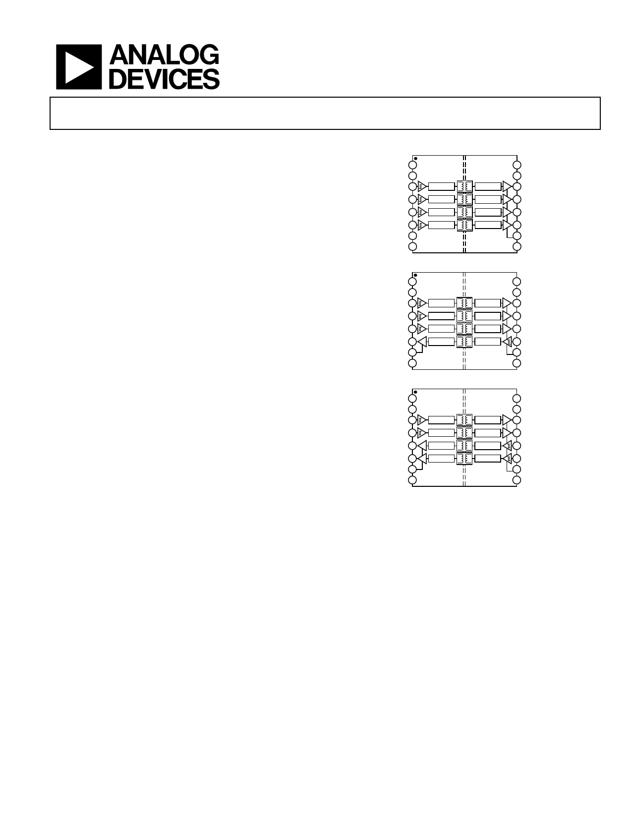
FUNCTIONAL BLOCK DIAGRAMS
VDD1 1
GND1 2
VIA 3
ENCODE
ADuM3440 16 VDD2
15 GND2
DECODE
14 VOA
VIB 4
ENCODE
DECODE
13 VOB
VIC 5
ENCODE
DECODE
12 VOC
VID 6
NC 7
GND1 8
ENCODE
DECODE
11 VOD
10 VE2
9 GND2
Figure 1. ADuM3440 Functional Block Diagram
VDD1 1
GND1 2
VIA 3
ENCODE
ADuM3441 16 VDD2
15 GND2
DECODE
14 VOA
VIB 4
ENCODE
DECODE
13 VOB
VIC 5
ENCODE
DECODE
12 VOC
VOD 6
VE1 7
GND1 8
DECODE
ENCODE
11 VID
10 VE2
9 GND2
Figure 2. ADuM3441 Functional Block Diagram
VDD1 1
GND1 2
VIA 3
VIB 4
ENCODE
ENCODE
ADuM3442 16 VDD2
15 GND2
DECODE
14 VOA
DECODE
13 VOB
VOC 5
DECODE
ENCODE
12 VIC
VOD 6
VE1 7
GND1 8
DECODE
ENCODE
11 VID
10 VE2
9 GND2
Figure 3. ADuM3442 Functional Block Diagram
Furthermore, iCoupler devices consume one-tenth to one-sixth
the power of optocouplers at comparable signal data rates.
The ADuM344x isolators provide four independent isolation
channels in a variety of channel configurations (see the
Ordering Guide). The ADuM344x operates with the supply
voltage on either side ranging from 3.0 V to 5.5 V, providing
compatibility with lower voltage systems as well as enabling
voltage translation functionality across the isolation barrier. In
addition, the ADuM344x provides low pulse width distortion
and tight channel-to-channel matching. Unlike other opto-
coupler alternatives, the ADuM344x isolators have a patented
refresh feature that ensures dc correctness in the absence of
input logic transitions and during the power-up/power-down
condition.
One Technology Way, P.O. Box 9106, Norwood, MA 02062-9106, U.S.A.
Tel: 781.329.4700
www.analog.com
Fax: 781.461.3113 ©2007–2012 Analog Devices, Inc. All rights reserved.
1 page 
Data Sheet
ADuM3440/ADuM3441/ADuM3442
ELECTRICAL CHARACTERISTICS—3.3 V OPERATION
All voltages are relative to their respective ground. 3.0 V ≤ VDD1 ≤ 3.6 V, 3.0 V ≤ VDD2 ≤ 3.6 V. All minimum/maximum specifications apply
over the entire recommended operation range, unless otherwise noted. All typical specifications are at TA = 25°C, VDD1 = VDD2 = 3.3 V.
Table 2.
Parameter
DC SPECIFICATIONS
Input Supply Current per Channel, Quiescent
Output Supply Current per Channel, Quiescent
ADuM3440, Total Supply Current, Four Channels1
DC to 2 Mbps
VDD1 Supply Current
VDD2 Supply Current
150 Mbps
VDD1 Supply Current
VDD2 Supply Current
ADuM3441, Total Supply Current, Four Channels1
DC to 2 Mbps
VDD1 Supply Current
VDD2 Supply Current
150 Mbps
VDD1 Supply Current
VDD2 Supply Current
ADuM3442, Total Supply Current, Four Channels1
DC to 2 Mbps
VDD1 or VDD2 Supply Current
150 Mbps
VDD1 or VDD2 Supply Current
For All Models
Input Currents
Logic High Input Threshold
Logic Low Input Threshold
Logic High Output Voltages
Symbol
IDDI (Q)
IDDO (Q)
IDD1 (Q)
IDD2 (Q)
IDD1 (150)
IDD2 (150)
IDD1 (Q)
IDD2 (Q)
IDD1 (150)
IDD2 (150)
IDD1 (Q), IDD2 (Q)
I , IDD1 (150) DD2 (150)
IIA, IIB, IIC,
IID, IE1, IE2
VIH, VEH
VIL, VEL
VOAH, VOBH,
VOCH, VODH
Logic Low Output Voltages
VOAL, VOBL,
VOCL, VODL
SWITCHING SPECIFICATIONS
Minimum Pulse Width2
Maximum Data Rate3
Propagation Delay4
Pulse Width Distortion, |tPLH − tPHL|4
Change vs. Temperature
Propagation Delay Skew5
Channel-to-Channel Matching,
Codirectional Channels6
Channel-to-Channel Matching,
Opposing Directional Channels5
PW
tPHL, tPLH
PWD
tPSK
tPSKCD
tPSKOD
Min Typ
0.43
0.3
1.7
1.2
63
17
1.6
1.3
52
29
1.5
40
−10 +0.01
1.6
(VDD1 or
VDD2) − 0.1
(VDD1 or
VDD2) − 0.4
3.0
2.8
0.0
0.04
0.2
150
20
0.5
3
Max
0.90
0.60
2.4
1.7
110
25
2.2
1.9
80
40
2.0
66
+10
0.4
0.1
0.1
0.4
6.67
36
2
16
2
5
Unit
mA
mA
mA
mA
mA
mA
mA
mA
mA
mA
mA
mA
µA
V
V
V
V
V
V
V
ns
Mbps
ns
ns
ps/°C
ns
ns
ns
Test Conditions
DC to 1 MHz logic signal frequency
DC to 1 MHz logic signal frequency
75 MHz logic signal frequency
75 MHz logic signal frequency
DC to 1 MHz logic signal frequency
DC to 1 MHz logic signal frequency
75 MHz logic signal frequency
75 MHz logic signal frequency
DC to 1 MHz logic signal frequency
75 MHz logic signal frequency
0 ≤ VIA, VIB, VIC, VID ≤ VDD1 or VDD2,
0 ≤ VE1, VE2 ≤ VDD1 or VDD2
IOx = −20 µA, VIx = VIxH
IOx = −4 mA, VIx = VIxH
IOx = 20 µA, VIx = VIxL
IOx = 400 µA, VIx = VIxL
IOx = 4 mA, VIx = VIxL
CL = 15 pF, CMOS signal levels
CL = 15 pF, CMOS signal levels
CL = 15 pF, CMOS signal levels
CL = 15 pF, CMOS signal levels
CL = 15 pF, CMOS signal levels
CL = 15 pF, CMOS signal levels
CL = 15 pF, CMOS signal levels
CL = 15 pF, CMOS signal levels
Rev. D | Page 5 of 24
5 Page 
Data Sheet
ADuM3440/ADuM3441/ADuM3442
DIN V VDE V 0884-10 (VDE V 0884-10) INSULATION CHARACTERISTICS
These isolators are suitable for reinforced electrical isolation only within the safety limit data. Maintenance of the safety data is ensured by
protective circuits. The asterisk (*) marking on packages denotes DIN V VDE V 0884-10 approval.
Table 7.
Description
Installation Classification per DIN VDE 0110
For Rated Mains Voltage ≤ 150 V rms
For Rated Mains Voltage ≤ 300 V rms
For Rated Mains Voltage ≤ 400 V rms
Climatic Classification
Pollution Degree per DIN VDE 0110, Table 1
Maximum Working Insulation Voltage
Input-to-Output Test Voltage, Method B1
Input-to-Output Test Voltage, Method A
After Environmental Tests Subgroup 1
After Input and/or Safety Test
Subgroup 2 and Subgroup 3
Highest Allowable Overvoltage
Safety-Limiting Values
Case Temperature
Side 1 Current
Side 2 Current
Insulation Resistance at TS
Conditions
VIORM × 1.875 = VPR, 100% production test, tm = 1 sec,
partial discharge < 5 pC
VIORM × 1.6 = VPR, tm = 60 sec, partial discharge < 5 pC
VIORM × 1.2 = VPR, tm = 60 sec, partial discharge < 5 pC
Transient overvoltage, tTR = 10 seconds
Maximum value allowed in the event of a failure
(see Figure 4)
VIO = 500 V
Symbol
VIORM
VPR
VPR
VTR
TS
IS1
IS2
RS
Characteristic
I to IV
I to III
I to II
40/105/21
2
560
1050
896
672
4000
150
265
335
>109
Unit
V peak
V peak
V peak
V peak
V peak
°C
mA
mA
Ω
350
300
250
SIDE #2
200
150
SIDE #1
100
50
0
0 50 100 150 200
CASE TEMPERATURE (°C)
Figure 4. Thermal Derating Curve, Dependence of Safety-Limiting Values
with Case Temperature per DIN V VDE V 0884-10
RECOMMENDED OPERATING CONDITIONS
Table 8.
Parameter
Rating
Operating Temperature Range, TA
Supply Voltage Range, VDD1, VDD21
Input Signal Rise and Fall Time
−40°C to +105°C
3.0 V to 5.5 V
1.0 ms
1 All voltages are relative to their respective ground. See the DC Correctness
and Magnetic Field Immunity section for information on immunity to external
magnetic fields.
Rev. D | Page 11 of 24
11 Page | ||
| Páginas | Total 24 Páginas | |
| PDF Descargar | [ Datasheet ADUM3441.PDF ] | |
Hoja de datos destacado
| Número de pieza | Descripción | Fabricantes |
| ADUM3440 | (ADUM3440 - ADUM3442) Quad Channel High Speed Digital Isolators | Analog Devices |
| ADUM3441 | (ADUM3440 - ADUM3442) Quad Channel High Speed Digital Isolators | Analog Devices |
| ADUM3442 | (ADUM3440 - ADUM3442) Quad Channel High Speed Digital Isolators | Analog Devices |
| Número de pieza | Descripción | Fabricantes |
| SLA6805M | High Voltage 3 phase Motor Driver IC. |
Sanken |
| SDC1742 | 12- and 14-Bit Hybrid Synchro / Resolver-to-Digital Converters. |
Analog Devices |
|
DataSheet.es es una pagina web que funciona como un repositorio de manuales o hoja de datos de muchos de los productos más populares, |
| DataSheet.es | 2020 | Privacy Policy | Contacto | Buscar |