|
|
|
PDF CLC1003 Data sheet ( Hoja de datos )
| Número de pieza | CLC1003 | |
| Descripción | RRIO Amplifier | |
| Fabricantes | Cadeka | |
| Logotipo | ||
Hay una vista previa y un enlace de descarga de CLC1003 (archivo pdf) en la parte inferior de esta página. Total 16 Páginas | ||
|
No Preview Available !
Data Sheet
Amplify the Human Experience
Comlinear® CLC1003
Low Distortion, Low Offset, RRIO Amplifier
www.datasheet4u.com
features
n 1mV max input offset voltage
n 0.00005% THD at 1kHz
n 5.3nV/√Hz input voltage noise >10kHz
n -90dB/-85dB HD2/HD3 at 100kHz, RL=100Ω
n <-100dB HD2 and HD3 at 10kHz, RL=1kΩ
n Rail-to-Rail input and output
n 55MHz unity gain bandwidth
n 12V/μs slew rate
n +80mA, -55mA output current
n -40°C to +125°C operating temperature
range
n Fully specified at 3V and ±5V supplies
n CLC1003: Pb-free SOT23-5, SOIC-8
n Future option CLC2003: Dual
n Future option CLC4003: Quad
Applications
n Active filters
n Sensor interface
n High-speed transducer amp
n Medical instrumentation
n Probe equipment
n Test equipment
n Smoke detecters
n Hand-held analytic instruments
General Description
The COMLINEAR CLC1003 is a single channel, high-performance, voltage
feedback amplifier with near precision performance, low input voltage noise,
and ultra low distortion. The CLC1003 family of amplifiers offers 1mV maxi-
mum input offset voltage, 3.5nV/√Hz broadband input voltage noise, and
0.00005% THD at 1kHz. These amplifiers also provide 55MHz gain bandwidth
product and 12V/μs slew rate making them well suited for applications requir-
ing precision DC performance and high AC performance. These COMLINEAR
high-performance amplifiers also offer a rail-to-rail input and output, simplify-
ing single supply designs and offering larger dynamic range possibilities. The
inputs extend beyond the rails by 500mV.
The COMLINEAR CLC1003 family of amplifiers are designed to operate from
2.5V to 12V supplies and operate over the extended temperature range of
-40°C to +125°.
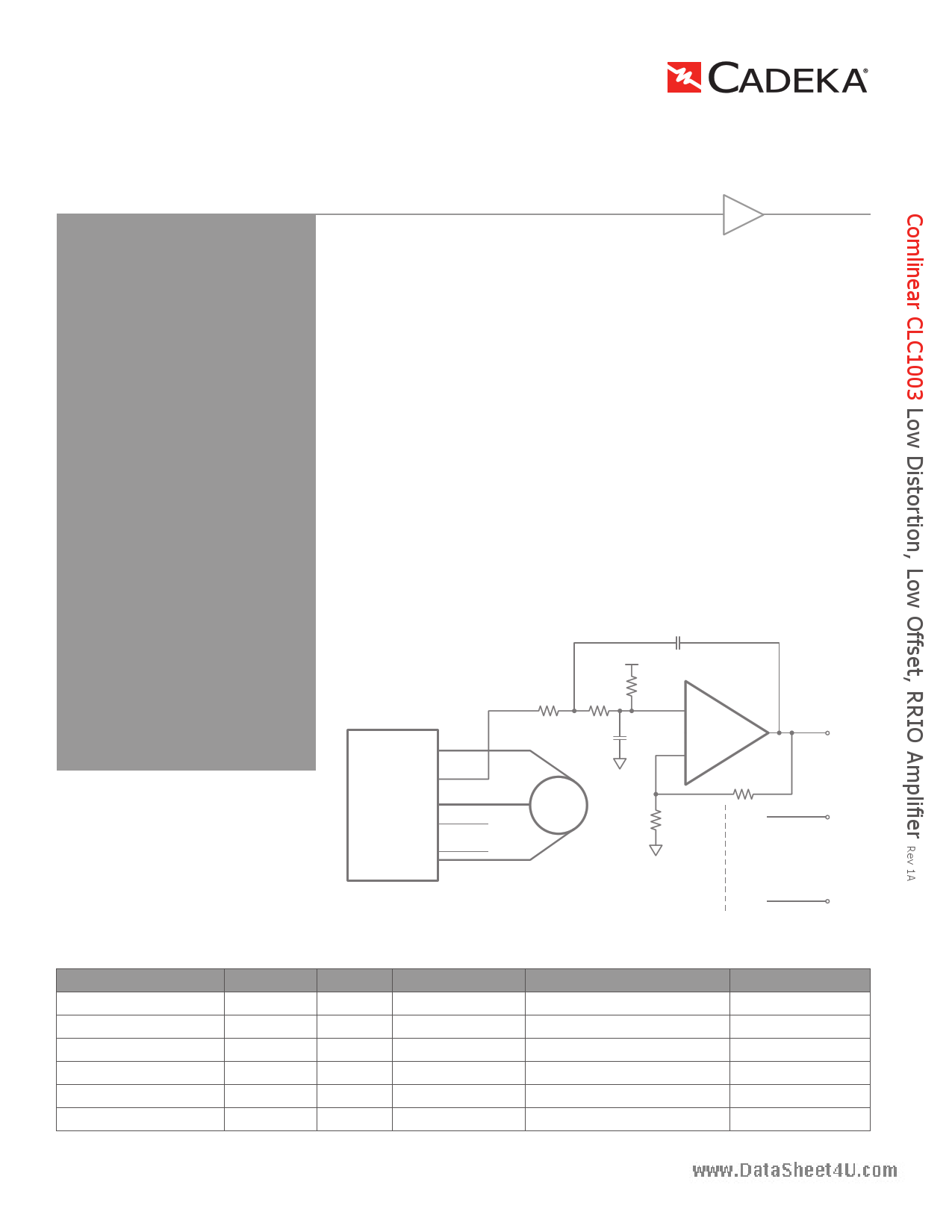
Typical Application - Current Sensing in 3-Phase Motor
SPM
(Smart
Power
Module)
VCC
M
+
CLC1003
–
lph_1
lph_2
lph_3
Ordering Information
Part Number
Package
CLC1003IST5X
SOT23-5
CLC1003ISO8X*
SOIC-8
CLC1003ISO8*
SOIC-8
CLC1003AST5X
SOT23-5
CLC1003ASO8X*
SOIC-8
CLC1003ASO8*
SOIC-8
*Preliminary Product Information
Moisture sensitivity level for all parts is MSL-1.
©2008 CADEKA Microcircuits LLC
Pb-Free
Yes
Yes
Yes
Yes
Yes
Yes
RoHS Compliant
Yes
Yes
Yes
Yes
Yes
Yes
Operating Temperature Range
-40°C to +85°C
-40°C to +85°C
-40°C to +85°C
-40°C to +125°C
-40°C to +125°C
-40°C to +125°C
Packaging Method
Reel
Reel
Rail
Reel
Reel
Rail
www.cadeka.com
1 page 
Data Sheet
Electrical Characteristics at ±5V
TA = 25°C, Vs = ±5V, Rf = 1kΩ, RL = 1kΩ to GND, G = 2; unless otherwise noted.
Symbol Parameter
Frequency Domain Response
GBWP
-3dB Gain Bandwidth Product
wwwU.dGaBtWasheet4u.Uconmity Gain Bandwidth
BWSS
-3dB Bandwidth
BWLS
Large Signal Bandwidth
Time Domain Response
tR, tF
tS
OS
Rise and Fall Time
Settling Time to 0.1%
Overshoot
SR Slew Rate
Distortion/Noise Response
HD2 2nd Harmonic Distortion
HD3 3rd Harmonic Distortion
THD Total Harmonic Distortion
en Input Voltage Noise
DC Performance
VIO
dVIO
Ib
dIb
Ios
PSRR
Input Offset Voltage(1)
Average Drift
Input Bias Current (1)
Average Drift
Input Offset Current (1)
Power Supply Rejection Ratio (1)
AOL Open-Loop Gain (1)
IS Supply Current (1)
Input Characteristics
RIN Input Resistance
CIN Input Capacitance
CMIR
Common Mode Input Range
CMRR
Common Mode Rejection Ratio (1)
Output Characteristics
Conditions
G = 10, VOUT = 0.05Vpp
VOUT = 0.05Vpp , Rf = 0
VOUT = 0.05Vpp
VOUT = 2Vpp
VOUT = 2V step; (10% to 90%)
VOUT = 2V step
VOUT = 2V step
4V step
2Vpp, 10kHz, RL = 1kΩ
2Vpp, 100kHz, RL = 100Ω
2Vpp, 10kHz, RL = 1kΩ
2Vpp, 100kHz, RL = 100Ω
1Vpp, 1kHz, G=1, RL = 2kΩ
> 10kHz
> 100kHz
DC
VOUT = VS / 2
per channel
Non-inverting, G = 1
DC , Vcm= -3V to 3V
VOUT
Output Voltage Swing
RL = 150Ω
RL = 1kΩ (1)
IOUT Output Current
ISC Short-Circuit Output Current
VOUT = VS / 2
Notes:
1. 100% tested at 25°C
Min Typ Max Units
35 MHz
55 MHz
25 MHz
3.6 MHz
125 ns
80 ns
0.3 %
12 V/µs
-125
-90
-127
-85
0.00005
5.3
3.5
dBc
dBc
dBc
dBc
%
nV/√Hz
nV/√Hz
-1 0.050
1
mV
1.3 µV/°C
-2.6 -0.30
2.6
μA
0.85 nA/°C
0.2 0.7 μA
82 100
dB
95 115
dB
2.2 2.75 mA
30
1
±5.5
70 95
MΩ
pF
V
dB
-4.826
to 4.534
-4.7 -4.93 to
4.85
+80, -55
+115, -90
4.7
V
V
mA
mA
©2004-2008 CADEKA Microcircuits LLC
www.cadeka.com 5
5 Page 
Data Sheet
Typical Performance Characteristics - Continued
TA = 25°C, Vs = ±5V, Rf = 1kΩ, RL = 1kΩ to GND, G = 2; unless otherwise noted.
Small Signal Pulse Response
0.75
www.datasheet4u.com
0.5
Small Signal Pulse Response at VS = 3V
1.65
1.6
0.25 1.55
0 1.5
-0.25
1.45
-0.5 1.4
-0.75
0
0.5 1 1.5
Time (ns)
2
1.35
0
0.5 1 1.5
Time (ns)
Large Signal Pulse Response
6
Large Signal Pulse Response at VS = 3V
3
4 2.5
22
0 1.5
-2 1
-4 0.5
-6
0 1 2 3 4 5 6 7 8 9 10
Time (ns)
0
0 0.5 1 1.5
Time (ns)
Input Offset Voltage vs. Temperature
0.1
Input Offset Voltage Distribution
5000
0.05
0
-0.05
-0.1
-0.15
-0.2
-40 -20
0
20 40 60 80 100 120
Temperature (°C)
4000
3000
2000
1000
0
Input Offset Voltage (mV)
2
2
©2004-2008 CADEKA Microcircuits LLC
www.cadeka.com 11
11 Page | ||
| Páginas | Total 16 Páginas | |
| PDF Descargar | [ Datasheet CLC1003.PDF ] | |
Hoja de datos destacado
| Número de pieza | Descripción | Fabricantes |
| CLC1001 | Ultra-Low Noise Amplifier | Cadeka |
| CLC1002 | Ultra-Low Noise Amplifier | Cadeka |
| CLC1003 | RRIO Amplifier | Cadeka |
| CLC1004 | (CLC1004 / CLC1014 / CLC3004) 750MHz Amplifiers | Cadeka |
| Número de pieza | Descripción | Fabricantes |
| SLA6805M | High Voltage 3 phase Motor Driver IC. |
Sanken |
| SDC1742 | 12- and 14-Bit Hybrid Synchro / Resolver-to-Digital Converters. |
Analog Devices |
|
DataSheet.es es una pagina web que funciona como un repositorio de manuales o hoja de datos de muchos de los productos más populares, |
| DataSheet.es | 2020 | Privacy Policy | Contacto | Buscar |