|
|
|
PDF ACS8595 Data sheet ( Hoja de datos )
| Número de pieza | ACS8595 | |
| Descripción | Line Card Protection Switch | |
| Fabricantes | Semtech Corporation | |
| Logotipo | ||
Hay una vista previa y un enlace de descarga de ACS8595 (archivo pdf) en la parte inferior de esta página. Total 12 Páginas | ||
|
No Preview Available !
ACS8595 ATCA
Line Card Protection Switch for
SONET/SDH AdvancedTCA Systems
ADVANCED COMMUNICATIONS
FINAL
PRODUCT BRIEF
Deswcwrwi.pDattiaoSnheet4U.com
Features
The ACS8595 ATCA is a highly integrated, single-chip
solution for “Hit-less” protection switching of SEC
(SDH/SONET Equipment Clock) + Sync clock “Groups”,
from Master and Slave SETS clock cards and a third
(Stand-by) source, for line cards/blades in a SONET or
SDH ATCA (Advanced Telecommuncications Computing
Architecture) Network Element. The ACS8595 has fast
activity monitors on the SEC clock inputs and will
implement automatic system protection switching against
the Master clock failure. The selection of the
Master/Slave input can be forced by a Force Fast Switch
pin. If both the Master and Slave input clocks fail, the
Stand-by “Group” is selected or, if no Stand-by is
available, the device enters Digital Holdover mode.
The ACS8595 can perform frequency translation,
converting, for example, an 8 kHz SEC input clock from
the ATCA backplane into a range of spot frequencies from
2 kHz up to 311.04 MHz (up to 77.76 MHz on the
TTL/CMOS ports). The output frequency is independently
programmable on each of the six SEC output ports, so the
ACS8595 ATCA has the potential to supply simultanously
up to six different SEC frequencies, for example, to meet
the individual requirements of several Advanced
Mezzanine Cards (AMCs).
The ACS8595 has one PECL/LVDS output port and five
TTL/CMOS ports. It also provides an 8 kHz Frame Sync
and a 2 kHz Multi-Frame Sync TTL/CMOS signal output
with programmable pulse width and polarity.
The ACS8595 includes a Serial Port, which can be SPI
compatible, providing access to the configuration and
status registers for device setup.
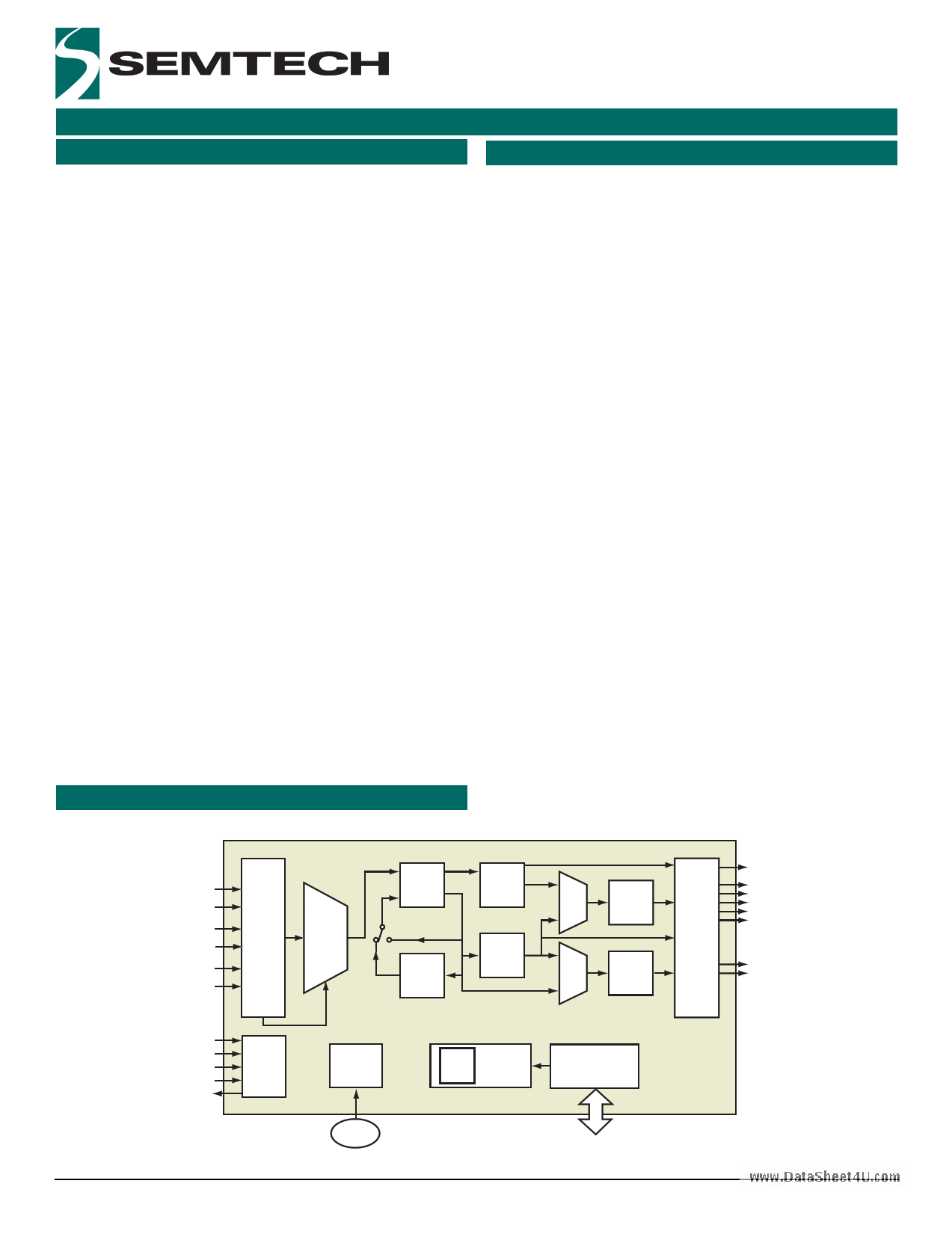
Block Diagram
SONET/SDH applications up to OC-3/STM-1 bit rates
Switches between grouped inputs (SEC/Sync pairs)
Inputs: three SECs at any of 2, 4, 8 kHz (and N x 8 kHz
multiples up to 155.52 MHz), plus Frame Sync/Multi-
Frame Sync
Outputs: Six SEC clocks at any of several spot frequen-
cies from 2 kHz up to 77.76 MHz via the TTL/CMOS
port and up to 311.04 MHz via the PECL/LVDS port
Modes for E3/DS3 and multiple E1/DS1 rate output
clocks
Generates 8 kHz Frame Sync and 2 kHz Multi-Frame
Sync output clocks with programmable pulse width
and polarity
Frequency translation of SEC input clock to different
local line card clocks
Robust activity monitoring on all clock inputs
Supports Free-run, Locked and Digital Holdover
modes of operation
Automatic “Hit-less” source switchover on loss of
input
External force fast switch between SEC1/SEC2 inputs
Phase Build-out for output clock phase continuity dur-
ing input switchover
PLL “Locked” and “Acquisition” bandwidths individu-
ally selectable from 18, 35 or 70 Hz
Serial interface for device set-up
IEEE 1149.1 JTAG Boundary Scan is supported.
Single 3.3 V operation, 5 V I/O compatible
Operating temperature (ambient) of -40 to +85°C
Available in 100-pin LQFP package
Lead (Pb)-free version (ACS8595T), RoHS and WEEE
compliant
Figure 1 Block Diagram of the ACS8595 ATCA
3 x SEC/Sync Input Groups
SEC1 & SEC2:
TTL/PECL/LVDS,
SEC3 and all Syncs
TTL only
SEC1
Master
SYNC1
Slave
SEC2
SYNC2
SEC3
Stand-by
SYNC3
SEC Inputs:
Programmable
Frequencies
2 kHz, 4 kHz,
N x 8 kHz
1.544/2.048 MHz
6.48 MHz
19.44 MHz
25.92 MHz
38.88 MHz
51.84 MHz
77.76 MHz
155.52 MHz
TCK
TDI
TMS
TRST
TDO
Input
SEC Port
Monitors
and
Input
Selection
Control
IEEE
1149.1
JTAG
Selector
DPLL1
DPLL2
Digital Feedback
APLL3
E1/DS1
Synthesis
Chip
Clock
Generator
TCXO or
XO
Priority Register Set
Table
MUX
2
MUX
1
APLL2
APLL 1
Output
Port
Frequency
Selection
Serial Interface
Port
SEC Outputs:
O1 (PECL/LVDS)
O2 (TTL)
O3 (TTL)
O4 (TTL)
O5 (TTL)
O6 (TTL)
Sync Outputs:
MFrSync 2 kHz (TTL)
FrSync 8 kHz (TTL)
01 TO O6:
8 kHz
1.544/2.048 MHz
3.088/4.096 MHz
6.176/8.192 MHz
12.352/16.384 MHz
6.48 MHz (not O1)
19.44 MHz
25.92 MHz
34.368 MHz
38.88 MHz
44.736 MHz
77.76 MHz
155.52 MHz (only O1)
311.04 MHz (only O1)
F8595_001BlockDia_01
Revision 2.00/October 2005 © Semtech Corp.
Page 1
www.semtech.com
1 page 
ACS8595 ATCA
ADVANCED COMMUNICATIONS
FINAL
PRODUCT BRIEF
Persiwswtewn.DtaatanSohmeeat4lUie.csocmause the alarm setting threshold to
be crossed and result in the selected SEC (and Sync)
being rejected.
There is one Leaky Bucket Accumulator per SEC input.
Each Leaky Bucket Accumulator can be programmed with
a Bucket ID (0 to 3) which assigns to the Leaky Bucket the
corresponding Leaky Bucket Configuration (from four
available Configurations). Each Leaky Bucket
Configuration comprises the following programmable
parameters:
z Bucket size
the Register Descriptions in the datasheet for advanced
features and more information.
DPLL1 Main Features
z Multiple E1 and DS1 outputs supported
z Low jitter MFrSync (2 kHz) and FrSync (8 kHz) outputs
z Multiple phase loss and multiple phase detectors
z Direct PLL locking to common SONET/SDH input
frequencies or any multiple of 8 kHz
z Automatic mode switching between Free-run, Locked
and Digital Holdover modes (states)
z Alarm trigger (set threshold)
z Alarm clear (reset threshold)
z Leak rate (decay rate
Phase Locked Loops (PLLs)
Figure 1 shows the PLL circuitry which comprises two
Digital PLLs (DPLL1 and DPLL2), two output multiplying
and filtering Analog PLLs (APLL1 and APLL2), output
frequency dividers in an Output Port Frequency Selection
block, a Synthesis block, multiplexers MUX1 and MUX2,
and a feedback Analog PLL (APLL3). These functional
blocks and their interconnections are highly configurable,
via register control, providing a range of output
frequencies and a choice of levels of jitter performance.
z Fast detection on input failure and entry into Digital
Holdover mode (holds at the last good frequency
value)
z Frequency translation between input and output rates
via direct digital synthesis
z High accuracy digital architecture for stable PLL
dynamics combined with an APLL for low jitter final
output clocks
z Non-revertive mode
z Frame Sync pulse alignment
z Selectable automatic DPLL bandwidth control (auto
selects either Locked bandwidth, or Acquisition
bandwidth), or Locked DPLL bandwidth
z Two programmable bandwidth controls:
The DPLLs give a stable and consistent level of
performance that can be easily programmed for different
dynamic behavior or operating range. They are not
affected by operating conditions or silicon process
variations. Digital Synthesis is used to generate all
required SONET/SDH output frequencies. The digital logic
operates at 204.8 MHz that is multiplied up from the
external 12.800 MHz oscillator module. Hence the best
resolution of the output signals from the DPLLs is one
204.8 MHz cycle or 4.9 ns.
• Locked bandwidth: 18, 35 or 70 Hz
• Acquisition bandwidth: 18, 35 or 70 Hz
z Programmable damping factor, (For optional faster
locking and peaking control) Factors = 1.2, 2.5, 5, 10
or 20
z Programmable DPLL pull-in frequency range
z Phase Build-out on source switching (hit-less source
switching), on/off
z Freeze Phase Build-out, on/off
Both of the DPLLs’ outputs can be connected to
multiplying and filtering APLLs. The outputs of these
APLLs are divided making a number of frequencies
simultaneously available for selection at the output clock
ports. The various combinations of DPLL, APLL,
Multiplexer and divider configurations allow for
generation of a comprehensive set of frequencies, as
listed in Table 5 and Table 6.
DPLLs
DPLL2 Main Features
The main features of DPLL2 are:
z Always locked to DPLL1
z Single programmable bandwidth control: 18, 35 or
70 Hz
z Programmable damping factor, (For optional faster
locking and peaking control) Factors = 1.2, 2.5, 5, 10
or 20.
DPLL1 is the more feature rich of the two DPLLs. The main z Digital feedback, on/off
features of the two DPLLs are summarized here. Refer to z Output frequency selection
Revision 2.00/October 2005 © Semtech Corp.
Page 5
www.semtech.com
5 Page 
ACS8595 ATCA
ADVANCED COMMUNICATIONS
FINAL
PRODUCT BRIEF
Tablew 7wRwegi.stDeraMat pa (Scohnt.e..)e t 4 U . c o m
Register Name
RO = Read Only
R/W = Read/Write
Data Bit
7 (MSB)
6
5
4
3
2
1 0 (LSB)
cnfg_phase_offset (R/W) [7:0] 70 00
phase_offset_value [7:0]
[15:8] 71 00
phase_offset_value[15:8]
cnfg_PBO_phase_offset (R/W) 72 00
PBO_phase_offset
cnfg_phase_loss_fine_limit (R/W) 73 A2 fine_limit_en noact_ph_loss narrow_en
phase_loss_fine_limit
cnfg_phase_loss_coarse_limit
(R/W)
74 85 coarse_lim_ wide_range_ multi_ph_resp
phaseloss_en en
phase_loss_coarse_limit
cnfg_ip_noise_window (R/W)
76 06 ip_noise_
window_en
sts_current_phase (RO) [7:0] 77 00
current_phase[7:0]
[15:8] 78 00
current_phase[15:8]
cnfg_phase_alarm_timeout
(R/W)
79 32
timeout_value (in two-second intervals)
cnfg_sync_pulses (R/W)
7A 00 2k_8k_from_
DPLL2
8k_invert
8k_pulse
2k_invert
2k_pulse
cnfg_sync_phase (R/W)
7B 00 Indep_FrSync/ Sync_OC-N_
MFrSync
rates
Sync_phase_SYNC3
Sync_phase_SYNC2
Sync_phase_SYNC1
cnfg_sync_monitor (R/W)
7C 2B ph_offset_
ramp
Sync_monitor_limit
cnfg_interrupt (R/W)
7D 02
Interrupt
GPO_en
Interrupt
tristate_en
Interrupt
int_polarity
cnfg_protection(R/W)
7E 85
protection_value
Revision 2.00/October 2005 © Semtech Corp.
Page 11
www.semtech.com
11 Page | ||
| Páginas | Total 12 Páginas | |
| PDF Descargar | [ Datasheet ACS8595.PDF ] | |
Hoja de datos destacado
| Número de pieza | Descripción | Fabricantes |
| ACS8595 | Line Card Protection Switch | Semtech Corporation |
| Número de pieza | Descripción | Fabricantes |
| SLA6805M | High Voltage 3 phase Motor Driver IC. |
Sanken |
| SDC1742 | 12- and 14-Bit Hybrid Synchro / Resolver-to-Digital Converters. |
Analog Devices |
|
DataSheet.es es una pagina web que funciona como un repositorio de manuales o hoja de datos de muchos de los productos más populares, |
| DataSheet.es | 2020 | Privacy Policy | Contacto | Buscar |