|
|
|
PDF ADS8506 Data sheet ( Hoja de datos )
| Número de pieza | ADS8506 | |
| Descripción | 12-BIT 40-KSPS LOW POWER SAMPLING ANALOG-TO-DIGITAL CONVERTER | |
| Fabricantes | Burr-Brown Corporation | |
| Logotipo | ||
Hay una vista previa y un enlace de descarga de ADS8506 (archivo pdf) en la parte inferior de esta página. Total 28 Páginas | ||
|
No Preview Available !
BurrĆBrown Products
from Texas Instruments
ADS8506
SLAS484A – SEPTEMBER 2007 – REVISED OCTOBER 2007
12-BIT 40-KSPS LOW POWER SAMPLING ANALOG-TO-DIGITAL CONVERTER WITH
INTERNAL REFERENCE AND PARALLEL/SERIAL INTERFACE
FEATURES
1
•2 40-kHz Min Sampling Rate
• 4-V, 5-V, and ±10-V Input Ranges
• 73.9-dB SINAD with 10-kHz Input
• ±0.45 LSB Max INL
• ±0.45 LSB Max DNL, 12-Bit No Missing Codes
• ±5-mV BPZ, ±0.5 PPM/°C BPZ Drift
• SPI Compatible Serial Output With
Daisy-Chain (TAG) Feature
• Single 5-V Analog Supply
• Pin-Compatible With ADS7806 and 16-Bit
ADS7807/8507
• Uses Internal or External 2.5-V Reference
• Low Power Dissipation
– 24 mW Typ, 30 mW Max at 40 KSPS
• 50-μW Max Power Down Mode
• 28-Pin SO Package
• Full Parallel Interface
• 2's Comp or BTC Output Code
APPLICATIONS
• Industrial Process Control
• Test Equipment
• Medical Equipment
• Data Acquisition Systems
• Digital Signal Processing
• Instrumentation
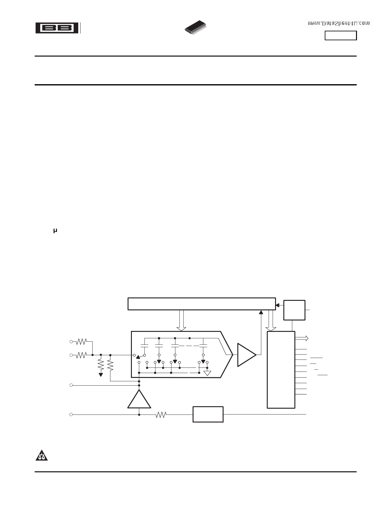
DESCRIPTION
The ADS8506 is a complete low power, single 5-V
supply, 12-bit sampling analog-to-digital (A/D)
converter. It contains a complete 12-bit
capacitor-based, successive approximation register
(SAR) A/D converter with sample and hold, clock,
reference, and data interface. The converter can be
configured for a variety of input ranges including ±10
V, 4 V, and 5 V. For most input ranges, the input
voltage can swing to 25 V or –25 V without damage
to the converter.
A SPI compatible serial interface allows data to be
synchronized to an internal or external clock. A full
parallel interface with BYTE select is also provided to
allow the maximum system design flexibility. The
ADS8506 is specified at 40 kHz sampling rate over
the industrial -40°C to 85°C temperature range.
Successive Approximation Register
Clock EXT/IN
R1IN
R2IN
39.8 kΩ
9.9 kΩ
20 kΩ
CAP
REF
40 kΩ
CDAC
Buffer
6 kΩ
Comparator
Parallel
and
Serial
Data
Out
&
Control
Internal
+2.5 V Ref
Parallel
Data
PWRD
BYTE
BUSY
CS
R/C
SB/BTC
TAG
SDATA
DATACLK
REFD
1
Please be aware that an important notice concerning availability, standard warranty, and use in critical applications of
Texas Instruments semiconductor products and disclaimers thereto appears at the end of this data sheet.
QSPI, SPI are trademarks of Motorola.
2
PRODUCTION DATA information is current as of publication date.
Products conform to specifications per the terms of the Texas
Instruments standard warranty. Production processing does not
necessarily include testing of all parameters.
Copyright © 2007, Texas Instruments Incorporated
1 page 
www.ti.com
TERMINAL
NO. NAME
1 R1IN
2 AGND1
3 R2IN
4 CAP
5 REF
6 AGND2
7 SB/BTC
8 EXT/INT
9 D7
10 D6
11 D5
12 D4
13 D3
14 DGND
15 D2
16 D1
17 D0
18 DATACLK
19 SDATA
20 TAG
21 BYTE
22 R/C
23 CS
24 BUSY
25 PWRD
26 REFD
27 VANA
28 VDIG
ADS8506
SLAS484A – SEPTEMBER 2007 – REVISED OCTOBER 2007
Terminal Functions
DIGITAL
I/O
I
I
O
O
O
O
O
O
O
O
I/O
O
I
I
I
I
O
I
I
DESCRIPTION
Analog Input.
Analog sense ground. Used internally as ground reference point. Minimal current flow
Analog Input.
Reference buffer output. 2.2-μF Tantalum capacitor to ground.
Reference input/output. Outputs internal 2.5-V reference. Can also be driven by external system
reference. In both cases, bypass to ground with a 2.2-μF tantalum capacitor.
Analog ground
Selects straight binary or binary 2's complement for output data format. if high, data is output in a
straight binary format. If low, data is output in a binary 2's complement format.
Selects external/Internal data clock for transmitting data. If high, data is output synchronized to
the clock input on DATACLK. If low, a convert command initiates the transmission of the data
from the previous conversion, along with 12-clock pulses output on DATACLK.
Data bit 3 if BYTE is high. Data bit 11 (MSB) if BYTE is low. Hi-Z when CS is high and/or R/C is
low. Leave unconnected when using serial output.
Data bit 2 if BYTE is high. Data bit 10 if BYTE is low. Hi-Z when CS is high and/or R/C is low.
Data bit 1 if BYTE is high. Data bit 9 if BYTE is low. Hi-Z when CS is high and/or R/C is low.
Data bit 0 (LSB) if BYTE is high. Data bit 8 if BYTE is low. Hi-Z when CS is high and/or R/C is
low.
Ground if BYTE is high. Data bit 7 if BYTE is low. Hi-Z when CS is high and/or R/C is low.
Digital ground
Ground if BYTE is high. Data bit 6 if BYTE is low. Hi-Z when CS is high and/or R/C is low.
Ground if BYTE is high. Data bit 5 if BYTE is low. Hi-Z when CS is high and/or R/C is low.
Ground if BYTE is high. Data bit 4 if BYTE is low. Hi-Z when CS is high and/or R/C is low.
Either an input or an output depending on the EXT/INT level. Output data is synchronized to this
clock. If EXT/INT is low, DATACLK transmits 12 pulses after each conversion, and then remains
low between conversions.
Serial data output. Data is synchronized to DATACLK, with the format determined by the level of
SB/BTC. In the external clock mode, after 12 bits of data, the ADC outputs the level input on
TAG as long as CS is low and R/C is high. If EXT/INT is low, data is valid on both the rising and
falling edges of DATACLK, and between conversions SDATA stays at the level of the TAG input
when the conversion was started.
Tag input for use in the external clock mode. If EXT is high, digital data input from TAG is output
on DATA with a delay that is dependent on the external clock mode.
Selects 8 most significant bits (low) or 8 least significant bits (high) on parallel output pins.
Read/convert input. With CS low, a falling edge on R/C puts the internal sample-and-hold into the
hold state and starts a conversion. When EXT/INT is low, this also initiates the transmission of
the data results from the previous conversion.
Internally ORed with R/C. If R/C is low, a falling edge on CS initiates a new conversion. If
EXT/INT is low, this same falling edge will start the transmission of serial data results from the
previous conversion.
At the start of a conversion, BUSY goes low and stays low until the conversion is completed and
the digital outputs have been updated.
Power down input. If high, conversions are inhibited and power consumption is significantly
reduced. Results from the previous conversion are maintained in the output shift register.
REFD High shuts down the internal reference. External reference will be required for
conversions.
Analog Supply. Nominally +5 V. Decouple with 0.1-μF ceramic and 10-μF tantalum capacitors.
Digital Supply. Nominally +5 V. Connect directly to pin 27. Must be ≤ VANA.
Copyright © 2007, Texas Instruments Incorporated
Product Folder Link(s): ADS8506
Submit Documentation Feedback
5
5 Page 
ADS8506
www.ti.com
SLAS484A – SEPTEMBER 2007 – REVISED OCTOBER 2007
LOW until the conversion is completed and the output register is updated. If BYTE (pin 21) is LOW, the eight
most significant bits (MSBs) will be valid when BUSY rises; if BYTE is HIGH, the four least significant bits (LSBs)
will be valid when BUSY rises. Data will be output in binary 2's complement (BTC) format. BUSY going HIGH
can be used to latch the data. After the first byte has been read, BYTE can be toggled allowing the remaining
byte to be read. All convert commands will be ignored while BUSY is LOW.
The ADS8506 begins tracking the input signal at the end of the conversion. Allowing 25 μs between convert
commands assures accurate acquisition of a new signal.
The offset and gain are adjusted internally to allow external trimming with a single supply. The external resistors
compensate for this adjustment and can be left out if the offset and gain will be corrected in software (refer to the
Calibration section).
± 10 V
+5 V
Parallel Output
200 Ω
1
28
66.5 kΩ
2.2 µF
2
3
100 Ω 4
2.2 µF
+5
6
27 +
+5 V
+
26 0.1 µF 10 µF
25
24 BUSY
23 Convert Pulse
7 ADS8506 22
8 21
9 20
R/C
BYTE
40 ns Min
10 19 NC(1)
11 18
12 17
13 16
14 15
Pin 21
LOW
Pin 21
HIGH
B11 B10 B9 B8 B7
(MSB)
B3 B2 B1 B0
(LSB)
B6 B5 B4
B2
Figure 31. Basic ±10-V Operation, Both Parallel and Serial Output
SERIAL OUTPUT
Figure 32 shows a basic circuit to operate the ADS8506 with a ±10-V input range and serial output. Taking R/C
(pin 22) LOW for 40 ns (12 μs max) will initiate a conversion and output valid data from the previous conversion
on SDATA (pin 19) synchronized to 12 clock pulses output on DATACLK (pin 18). BUSY (pin 24) will go LOW
and stay LOW until the conversion is completed and the serial data has been transmitted. Data will be output in
BTC format, MSB first, and will be valid on both the rising and falling edges of the data clock. BUSY going HIGH
can be used to latch the data. All convert commands will be ignored while BUSY is LOW.
The ADS8506 begins tracking the input signal at the end of the conversion. Allowing 25 μs between convert
commands assures accurate acquisition of a new signal.
The offset and gain are adjusted internally to allow external trimming with a single supply. The external resistors
compensate for this adjustment and can be left out if the offset and gain are corrected in software (refer to the
Calibration section).
Copyright © 2007, Texas Instruments Incorporated
Product Folder Link(s): ADS8506
Submit Documentation Feedback
11
11 Page | ||
| Páginas | Total 28 Páginas | |
| PDF Descargar | [ Datasheet ADS8506.PDF ] | |
Hoja de datos destacado
| Número de pieza | Descripción | Fabricantes |
| ADS850 | ADS850: 14-Bit 10 MSPS Self-Calibrating Analog-to-Digital Converter (Rev. C) | Texas Instruments |
| ADS8504 | SAMPLING CMOS ANALOG-TO-DIGITAL CONVERTER | Burr-Brown |
| ADS8504 | 12-BIT 250-KSPS Sampling CMOS Analog-to-Digital Converter (Rev. A) | Texas Instruments |
| ADS8505 | 16-Bit 250-KSPS Sampling CMOS Analog-to-Digital Converter (Rev. B) | Texas Instruments |
| Número de pieza | Descripción | Fabricantes |
| SLA6805M | High Voltage 3 phase Motor Driver IC. |
Sanken |
| SDC1742 | 12- and 14-Bit Hybrid Synchro / Resolver-to-Digital Converters. |
Analog Devices |
|
DataSheet.es es una pagina web que funciona como un repositorio de manuales o hoja de datos de muchos de los productos más populares, |
| DataSheet.es | 2020 | Privacy Policy | Contacto | Buscar |