|
|
|
PDF EDS6432AFBH Data sheet ( Hoja de datos )
| Número de pieza | EDS6432AFBH | |
| Descripción | 64M bits SDRAM | |
| Fabricantes | Elpida Memory | |
| Logotipo | ||
Hay una vista previa y un enlace de descarga de EDS6432AFBH (archivo pdf) en la parte inferior de esta página. Total 30 Páginas | ||
|
No Preview Available !
DATA SHEET
64M bits SDRAM
EDS6432AFBH, EDS6432CFBH
(2M words × 32 bits)
Description
The EDS6432AFBH, EDS6432CFBH are 64M bits
SDRAMs organized as 524,288 words × 32 bits × 4
banks. All inputs and outputs are synchronized with
www.DataSheet4Ut.hcoempositive edge of the clock.
Supply voltages are 3.3V (EDS6432AFBH) and 2.5V
(EDS6432CFBH).
They are packaged in 90-ball FBGA.
Features
• 3.3V and 2.5V power supply
• Clock frequency: 166MHz/133MHz (max.)
• Single pulsed /RAS
• ×32 organization
• 4 banks can operate simultaneously and
independently
• Burst read/write operation and burst read/single
write operation capability
• Programmable burst length (BL): 1, 2, 4, 8, full page
• 2 variations of burst sequence
Sequential (BL = 1, 2, 4, 8, full page)
Interleave (BL = 1, 2, 4, 8)
• Programmable /CAS latency (CL): 2, 3
• Byte control by DQM
• Refresh cycles: 4096 refresh cycles/64ms
• 2 variations of refresh
Auto refresh
Self refresh
• FBGA package with lead free solder (Sn-Ag-Cu)
RoHS compliant
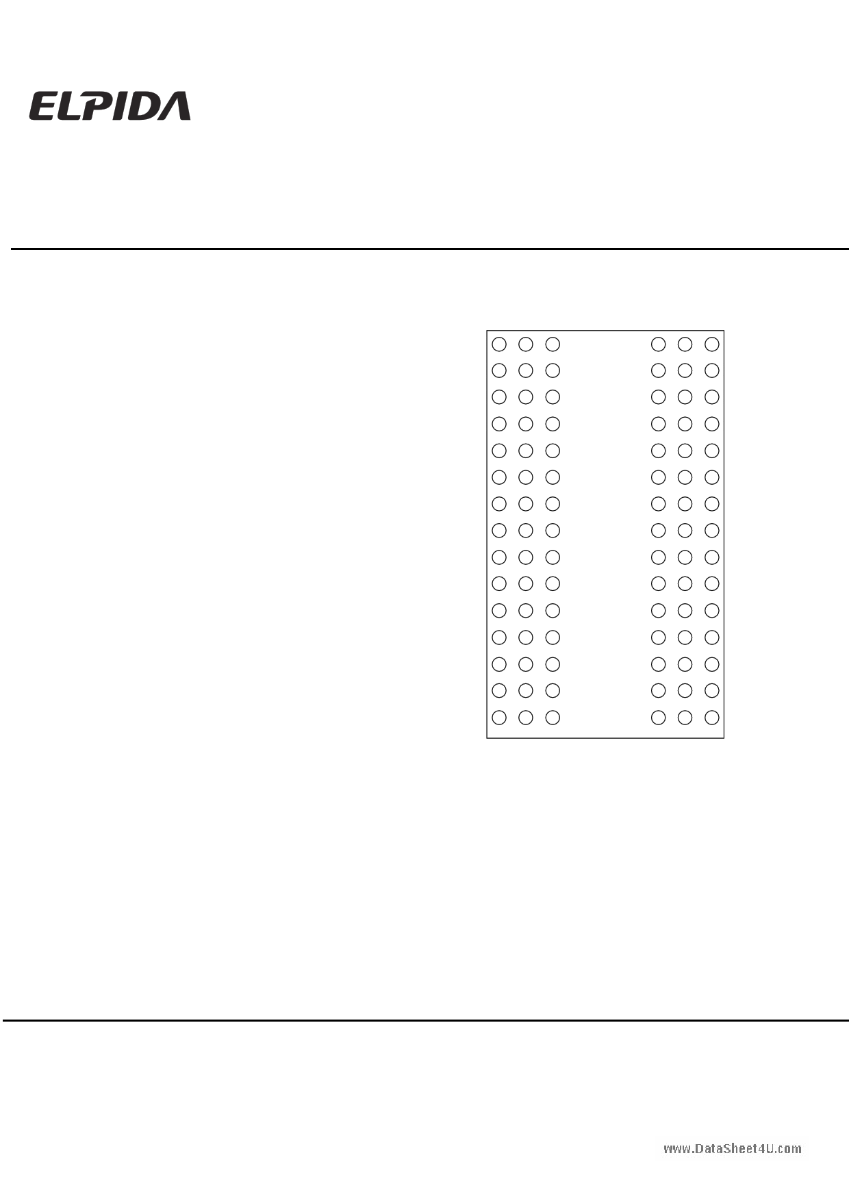
Pin Configurations
/xxx indicate active low signal.
90-ball FBGA
123456789
A
DQ26 DQ24 VSS
B
DQ28 VDDQ VSSQ
C
VSSQ DQ27 DQ25
D
VSSQ DQ29 DQ30
E
VDDQ DQ31 NC
F
VSS DQM3 A3
G
A4 A5 A6
H
A7 A8 NC
J
CLK CKE A9
K
DQM1 NC NC
L
VDDQ DQ8 VSS
M
VSSQ DQ10 DQ9
N
VSSQ DQ12 DQ14
P
DQ11 VDDQ VSSQ
R
DQ13 DQ15 VSS
(Top view)
VDD DQ23 DQ21
VDDQ VSSQ DQ19
DQ22 DQ20 VDDQ
DQ17 DQ18 VDDQ
NC DQ16 VSSQ
A2 DQM2 VDD
A10 A0 A1
NC BA1 NC
BA0 /CS /RAS
/CAS /WE DQM0
VDD DQ7 VSSQ
DQ6 DQ5 VDDQ
DQ1 DQ3 VDDQ
VDDQ VSSQ DQ4
VDD DQ0 DQ2
A0 to A10
BA0, BA1
DQ0 to DQ31
/CS
/RAS
/CAS
/WE
DQM0 to DQM3
CKE
CLK
VDD
VSS
VDDQ
VSSQ
NC
Address inputs
Bank select address
Data-input/output
Chip select
Row address strobe
Column address strobe
Write enable
DQ mask enable
Clock enable
Clock input
Power for internal circuit
Ground for internal circuit
Power for DQ circuit
Ground for DQ circuit
No connection
Document No. E0497E20 (Ver. 2.0)
Date Published July 2005 (K) Japan
Printed in Japan
URL: http://www.elpida.com
Elpida Memory, Inc. 2004-2005
1 page 
EDS6432AFBH, EDS6432CFBH
DC Characteristics 1 (TA = 0°C to +70°C, VDD, VDDQ = 3.3V ± 0.3V, VSS, VSSQ = 0V) [EDS6432AF]
(TA = 0°C to +70°C, VDD, VDDQ = 2.5V ± 0.2V, VSS, VSSQ = 0V) [EDS6432CF]
EDS6432AF EDS6432CF
Parameter
Symbol
Grade max.
max.
Unit Test condition
Notes
Operating current
IDD1
-6B 120
-75 100
120
100
mA
Burst length = 1
tRC = tRC (min.)
1, 2, 3
Standby current in power
down
IDD2P
3
3
mA
CKE = VIL,
tCK = tCK (min.)
6
Standby current in power
down (input signal stable)
IDD2PS
2 2 mA CKE = VIL, tCK = ∞ 7
Standby current in non power
down
IDD2N
20
20
mA
CKE, /CS = VIH,
tCK = tCK (min.)
4
Standby current in non power
down (input signal stable)
IDD2NS
9
9
mA
CKE = VIH, tCK = ∞,
/CS = VIH
8
Active standby current in
www.DataSheet4Up.coowmer down
IDD3P
4
4
mA
CKE = VIL,
tCK = tCK (min.)
1, 2, 6
Active standby current in
power down (input signal
stable)
IDD3PS
3 3 mA CKE = VIL, tCK = ∞ 2, 7
Active standby current in non
power down
IDD3N
40
40
mA
CKE, /CS = VIH,
tCK = tCK (min.)
1, 2, 4
Active standby current in non
power down (input signal
IDD3NS
stable)
30
30
mA
CKE = VIH, tCK = ∞,
/CS = VIH
2, 8
Burst operating current
IDD4
-6B 150
-75 130
150
130
mA
tCK = tCK (min.),
BL = 4
1, 2, 5
Refresh current
IDD5
-6B 260
-75 220
260
220
mA tRC = tRC (min.)
3
Self refresh current
IDD6
1.5
1.5
mA
VIH ≥ VDD – 0.2V
VIL ≤ 0.2V
Notes: 1. IDD depends on output load condition when the device is selected. IDD (max.) is specified at the output
open condition.
2. One bank operation.
3. Input signals are changed once per one clock.
4. Input signals are changed once per two clocks.
5. Input signals are changed once per four clocks.
6. After power down mode, CLK operating current.
7. After power down mode, no CLK operating current.
8. Input signals are VIH or VIL fixed.
Data Sheet E0497E20 (Ver. 2.0)
5
5 Page 
EDS6432AFBH, EDS6432CFBH
Pin Function
CLK (input pin)
CLK is the master clock input. Other inputs signals are referenced to the CLK rising edge.
CKE (input pins)
CKE determine validity of the next CLK (clock). If CKE is high, the next CLK rising edge is valid; otherwise it is
invalid. If the CLK rising edge is invalid, the internal clock is not issued and the Synchronous DRAM suspends
operation.
When the Synchronous DRAM is not in burst mode and CKE is negated, the device enters power down mode.
During power down mode, CKE must remain low.
/CS (input pins)
/CS low starts the command input cycle. When /CS is high, commands are ignored but operations continue.
www.DataSheet4U.com
/RAS, /CAS, and /WE (input pins)
/RAS, /CAS and /WE have the same symbols on conventional DRAM but different functions. For details, refer to the
command table.
A0 to A10 (input pins)
Row Address is determined by A0 to A10 at the CLK (clock) rising edge in the active command cycle.
Column Address is determined by A0 to A7 at the CLK rising edge in the read or write command cycle.
A10 defines the precharge mode. When A10 is high in the precharge command cycle, all banks are precharged;
when A10 is low, only the bank selected by BA0 and BA1 is precharged.
When A10 is high in read or write command cycle, the precharge starts automatically after the burst access.
BA0 and BA1 (input pin)
BA0 and BA1 are bank select signal (BS). (See Bank Select Signal Table)
[Bank Select Signal Table]
BA0
Bank 0
L
Bank 1
H
Bank 2
L
Bank 3
H
Remark: H: VIH. L: VIL.
BA1
L
L
H
H
DQM (input pins)
DQM controls I/O buffers. DQM0 controls DQ0 to DQ7, DQM1 controls DQ8 to DQ15, DQM2 controls DQ16 to
DQ23, DQM3 controls DQ24 to DQ31. In read mode, DQM controls the output buffers like a conventional /OE pin.
DQM high and DQM low turn the output buffers off and on, respectively. The DQM latency for the read is two clocks.
In write mode, DQM controls the word mask. Input data is written to the memory cell if DQM is low but not if DQM is
high. The DQM latency for the write is zero.
DQ0 to DQ31 (input/output pins)
DQ pins have the same function as I/O pins on a conventional DRAM.
VDD, VSS, VDDQ, VSSQ (Power supply)
VDD and VSS are power supply pins for internal circuits. VDDQ and VSSQ are power supply pins for the output
buffers.
Data Sheet E0497E20 (Ver. 2.0)
11
11 Page | ||
| Páginas | Total 30 Páginas | |
| PDF Descargar | [ Datasheet EDS6432AFBH.PDF ] | |
Hoja de datos destacado
| Número de pieza | Descripción | Fabricantes |
| EDS6432AFBH | 64M bits SDRAM | Elpida Memory |
| EDS6432AFBH | 64M bits SDRAM | Elpida Memory |
| EDS6432AFBH-TT | 64M bits SDRAM WTR | Elpida Memory |
| Número de pieza | Descripción | Fabricantes |
| SLA6805M | High Voltage 3 phase Motor Driver IC. |
Sanken |
| SDC1742 | 12- and 14-Bit Hybrid Synchro / Resolver-to-Digital Converters. |
Analog Devices |
|
DataSheet.es es una pagina web que funciona como un repositorio de manuales o hoja de datos de muchos de los productos más populares, |
| DataSheet.es | 2020 | Privacy Policy | Contacto | Buscar |