|
|
|
PDF ADL5375 Data sheet ( Hoja de datos )
| Número de pieza | ADL5375 | |
| Descripción | 400 MHz to 6 GHz Broadband Quadrature Modulator | |
| Fabricantes | Analog Devices | |
| Logotipo | ||
Hay una vista previa y un enlace de descarga de ADL5375 (archivo pdf) en la parte inferior de esta página. Total 30 Páginas | ||
|
No Preview Available !
400 MHz to 6 GHz
Broadband Quadrature Modulator
ADL5375
FEATURES
Output frequency range: 400 MHz to 6 GHz
1 dB output compression: ≥9.4 dBm from 450 MHz to 4 GHz
Output return loss ≤ 14 dB from 450 MHz to 5.5 GHz
Noise floor: −160 dBm/Hz @ 900 MHz
Sideband suppression: <−50 dBc @ 900 MHz
Carrier feedthrough: <−46 dBm @ 900 MHz
www.DataSheeBt4aUse.cboamnd input bias level
ADL5375-05: 500 mV
ADL5375-15: 1500 mV
Single supply: 4.75 V to 5.25 V
24-lead LFCSP_VQ package
APPLICATIONS
Cellular communication systems
GSM/EDGE, CDMA2000, W-CDMA, TD-SCDMA
WiMAX/broadband wireless access systems
Satellite modems
GENERAL DESCRIPTION
The ADL5375 is a broadband quadrature modulator designed for
operation from 400 MHz to 6 GHz. Its excellent phase accuracy
and amplitude balance enable high performance intermediate
frequency or direct radio frequency modulation for commu-
nication systems.
The ADL5375 features a broad baseband bandwidth, along
with an output gain flatness that varies no more than 1 dB
from 450 MHz to 3.8 GHz. These features, coupled with a broad-
band output return loss of ≤−14 dB, make the ADL5375 ideally
suited for broadband zero IF or low IF-to-RF applications,
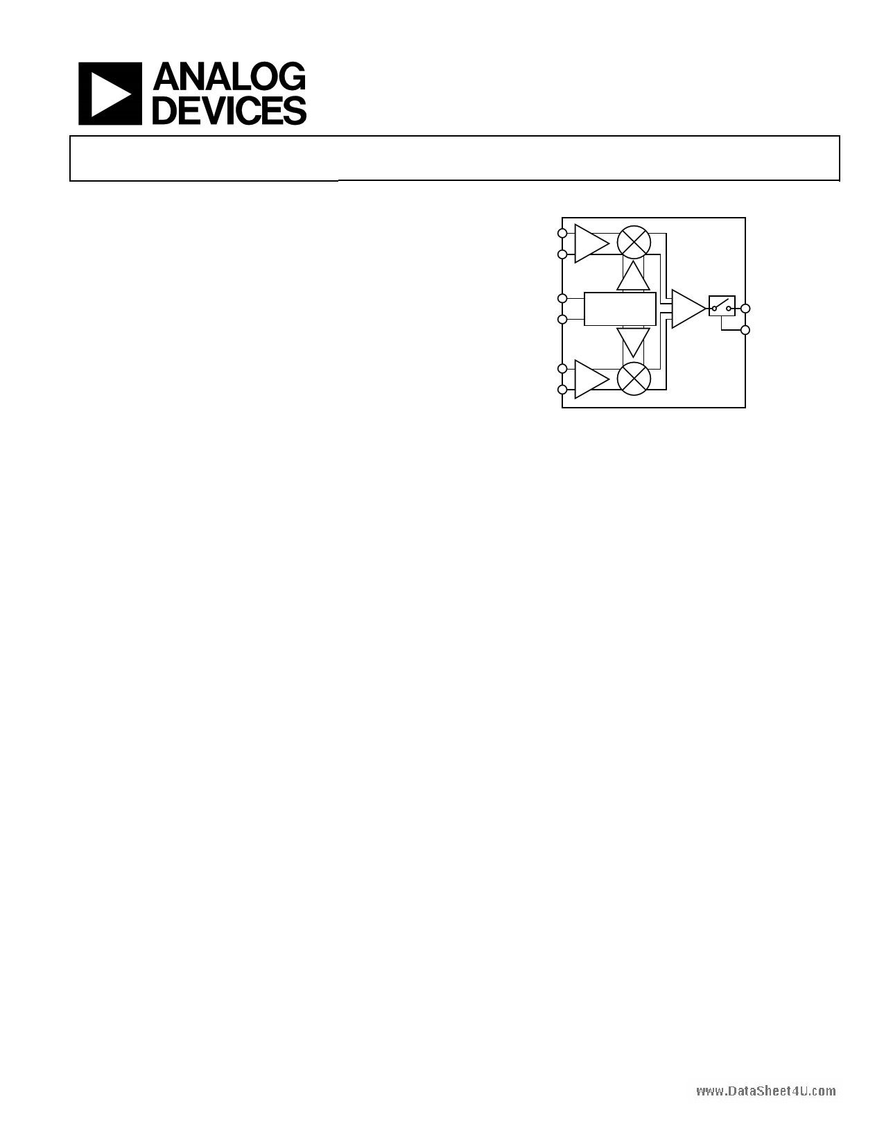
FUNCTIONAL BLOCK DIAGRAM
IBBP
IBBN
ADL5375
LOIP
LOIN
QUADRATURE
PHASE
SPLITTER
QBBN
QBBP
Figure 1.
RFOUT
DSOP
broadband digital predistortion transmitters, and multiband
radio designs.
The ADL5375 accepts two differential baseband inputs and
a single-ended LO. It generates a single-ended 50 Ω output.
The two versions offer input baseband bias levels of 500 mV
(ADL5375-05) and 1500 mV (ADL5375-15).
The ADL5375 is fabricated using an advanced silicon-germanium
bipolar process. It is available in a 24-lead, exposed paddle, Pb-free,
LFCSP_VQ package. Performance is specified over a −40°C to
+85°C temperature range. A Pb-free evaluation board is also
available.
Rev. 0
Information furnished by Analog Devices is believed to be accurate and reliable. However, no
responsibility is assumed by Analog Devices for its use, nor for any infringements of patents or other
rights of third parties that may result from its use. Specifications subject to change without notice. No
license is granted by implication or otherwise under any patent or patent rights of Analog Devices.
Trademarksandregisteredtrademarksarethepropertyoftheirrespectiveowners.
One Technology Way, P.O. Box 9106, Norwood, MA 02062-9106, U.S.A.
Tel: 781.329.4700
www.analog.com
Fax: 781.461.3113
©2007 Analog Devices, Inc. All rights reserved.
1 page 
Parameter
LO = 2600 MHz
Output Power, POUT
Modulator Voltage Gain
Output P1dB
Output Return Loss
Carrier Feedthrough
Sideband Suppression
Quadrature Error
I/Q Amplitude Balance
Second Harmonic
www.DataSheet4U.cAoDmL5375-05
ADL5375-15
Third Harmonic
ADL5375-05
ADL5375-15
Output IP2
Output IP3
Noise Floor
LO = 3500 MHz
Output Power, POUT
Modulator Voltage Gain
Output P1dB
Output Return Loss
Carrier Feedthrough
Sideband Suppression
Quadrature Error
I/Q Amplitude Balance
Second Harmonic
ADL5375-05
ADL5375-15
Third Harmonic
ADL5375-05
ADL5375-15
Output IP2
Output IP3
Noise Floor
ADL5375
Conditions
VIQ = 1 V p-p differential
RF output divided by baseband input voltage
POUT − (fLO + (2 × fBB))
POUT = 1.18 dBm
POUT = 0.78 dBm
POUT − (fLO + (3 × fBB))
POUT = 1.18 dBm
POUT = 0.78 dBm
f1BB = 3.5 MHz, f2BB = 4.5 MHz,
POUT ≈ −5 dBm @ fLO = 900 MHz
f1BB = 3.5 MHz, f2BB = 4.5 MHz,
POUT ≈ −5 dBm @ fLO = 900 MHz
I/Q inputs = 0 V differential with a dc bias
only, 20 MHz carrier offset
VIQ = 1 V p-p differential
RF output divided by baseband input voltage
POUT − (fLO + (2 × fBB))
POUT = 1.71 dBm
POUT = 1.14 dBm
POUT − (fLO + (3 × fBB))
POUT = 1.71 dBm
POUT = 1.14 dBm
f1BB = 3.5 MHz, f2BB = 4.5 MHz,
POUT ≈ −5 dBm @ fLO = 900 MHz
f1BB = 3.5 MHz, f2BB = 4.5 MHz,
POUT ≈ −5 dBm @ fLO = 900 MHz
I/Q inputs = 0 V differential with a dc bias
only, 20 MHz carrier offset
ADL5375-05
ADL5375-15
Min Typ Max Min Typ Max Unit
1.18
−2.8
10.3
−15.1
−41.0
−44.3
−0.72
−0.04
−57
0.78
−3.2
10.6
−14.5
−42.3
−45.6
−0.60
−0.07
−55
dBm
dB
dBm
dB
dBm
dBc
Degrees
dB
dBc
−52 −52 dBc
49.0
21.8
−159.0
48.5
19.4
−157.6
dBm
dBm
dBm/Hz
1.71
−2.3
10.4
−21.6
−30.5
−49.3
−0.20
−0.07
−54
1.14
−2.8
10.1
−20.4
−29.0
−44.9
−0.54
−0.08
−61
dBm
dB
dBm
dB
dBm
dBc
Degrees
dB
dBc
−53 −51 dBc
50.0
23.8
−157.6
57.9
19.5
−156.3
dBm
dBm
dBm/Hz
Rev. 0 | Page 5 of 32
5 Page 
ADL5375-05
0
SSB OUTPUT
–10 POWER (dBm)
–20
CARRIER
FEEDTHROUGH (dBm)
–30
10
5
–40 0
–50
–60 –5
SIDEBAND
–70 SUPPRESSION (dBc)
SECOND-ORDER
–80 DISTORTION (dBc) –10
www.DataSheet4U.co–m90
–100
0.06
THIRD-ORDER
DISTORTION (dBc)
0.1 1
BASEBAND INPUT VOLTAGE (V rms)
–15
2
Figure 15. Second- and Third-Order Distortion, Carrier Feedthrough,
Sideband Suppression, and SSB POUT vs. Baseband Differential Input Level
(fLO = 3500 MHz)
0
–10
–20
–30
–40
THIRD-ORDER
–50
TA = +25°C
TA = +85°C
TA = –40°C
–60 SECOND-ORDER
–70
–80
0
0.5 1.0 1.5 2.0 2.5 3.0 3.5 4.0 4.5 5.0 5.5 6.0
LO FREQUENCY (GHz)
Figure 16. Second- and Third-Order Distortion vs. LO Frequency (fLO) and
Temperature (Baseband I/Q Amplitude = 1 V p-p Differential)
–20
SSB OUTPUT POWER (dBm)
1.5
–30
CARRIER
0.5
FEEDTHROUGH (dBm)
–40 –0.5
–50 SIDEBAND
SUPPRESSION (dBc)
–1.5
–60 –2.5
–70
1
SECOND-ORDER
DISTORTION (dBc)
–3.5
10 100
BASEBAND FREQUENCY (MHz)
Figure 17. Second-Order Distortion, Carrier Feedthrough, Sideband
Suppression, and SSB POUT vs. Baseband Frequency (fBB); fLO = 2140 MHz
ADL5375
30
28
26
24
22
20
18
16
14
12
10
8
6
4
2
0
0
TA = –40°C
TA = +25°C
TA = +85°C
0.5 1.0 1.5 2.0 2.5 3.0 3.5 4.0 4.5 5.0 5.5 6.0
LO FREQUENCY (GHz)
Figure 18. OIP3 vs. LO Frequency (fLO) and Temperature (POUT ≈ −5 dBm @
fLO = 900 MHz)
80
70
60
TA = –40°C
50
40 TA = +25°C
30 TA = +85°C
20
10
0
0 0.5 1.0 1.5 2.0 2.5 3.0 3.5 4.0 4.5 5.0 5.5 6.0
LO FREQUENCY (GHz)
Figure 19. OIP2 vs. LO Frequency (fLO) and Temperature (POUT ≈ −5 dBm @
fLO = 900 MHz)
–20
SSB OUTPUT
POWER (dBm)
–30
CARRIER
–40 FEEDTHROUGH (dBm)
2
1
0
–50 –1
–60
SIDEBAND
SUPPRESSION (dBc)
THIRD-ORDER
DISTORTION (dBc)
–2
SECOND-ORDER
DISTORTION (dBc)
–70 –3
–80 –4
–6 –4 –2 0 2 4 6
LO AMPLITUDE (dBm)
Figure 20. Second- and Third-Order Distortion, Carrier Feedthrough,
Sideband Suppression, and SSB POUT vs. LO Amplitude (fLO = 900 MHz)
Rev. 0 | Page 11 of 32
11 Page | ||
| Páginas | Total 30 Páginas | |
| PDF Descargar | [ Datasheet ADL5375.PDF ] | |
Hoja de datos destacado
| Número de pieza | Descripción | Fabricantes |
| ADL5370 | Quadrature Modulator | Analog Devices |
| ADL5371 | 500 MHz to 1500 MHz Quadrature Modulator | Analog Devices |
| ADL5372 | (ADL5370 - ADL5374) Quadrature Modulator | Analog Devices |
| ADL5373 | (ADL5370 - ADL5374) Quadrature Modulator | Analog Devices |
| Número de pieza | Descripción | Fabricantes |
| SLA6805M | High Voltage 3 phase Motor Driver IC. |
Sanken |
| SDC1742 | 12- and 14-Bit Hybrid Synchro / Resolver-to-Digital Converters. |
Analog Devices |
|
DataSheet.es es una pagina web que funciona como un repositorio de manuales o hoja de datos de muchos de los productos más populares, |
| DataSheet.es | 2020 | Privacy Policy | Contacto | Buscar |