|
|
|
PDF DS12B887 Data sheet ( Hoja de datos )
| Número de pieza | DS12B887 | |
| Descripción | Real Time Clock | |
| Fabricantes | Dallas Semiconductor | |
| Logotipo | ||
Hay una vista previa y un enlace de descarga de DS12B887 (archivo pdf) en la parte inferior de esta página. Total 16 Páginas | ||
|
No Preview Available !
DS12B887
DS12B887
Real Time Clock
www.DataSheet4U.com
FEATURES
• Drop-in replacement for IBM AT computer clock/cal-
endar
• Pin compatible with the MC146818B and DS1287
• Totally nonvolatile with over 10 years of operation in
the absence of power
• Self-contained subsystem includes lithium, quartz,
and support circuitry
• Counts seconds, minutes, hours, days, day of the
week, date, month, and year with leap year com-
pensation
• Binary or BCD representation of time, calendar, and
alarm
• 12- or 24-hour clock with AM and PM in 12-hour mode
• Daylight Savings Time option
• Multiplex bus for pin efficiency
• Interfaced with software as 128 RAM locations
– 14 bytes of clock and control registers
– 114 bytes of general purpose RAM
• Programmable square wave output signal
• Bus-compatible interrupt signals (IRQ)
• Three interrupts are separately software-maskable
and testable
– Time-of-day alarm once/second to once/day
– Periodic rates from 122 µs to 500 ms
– End of clock update cycle
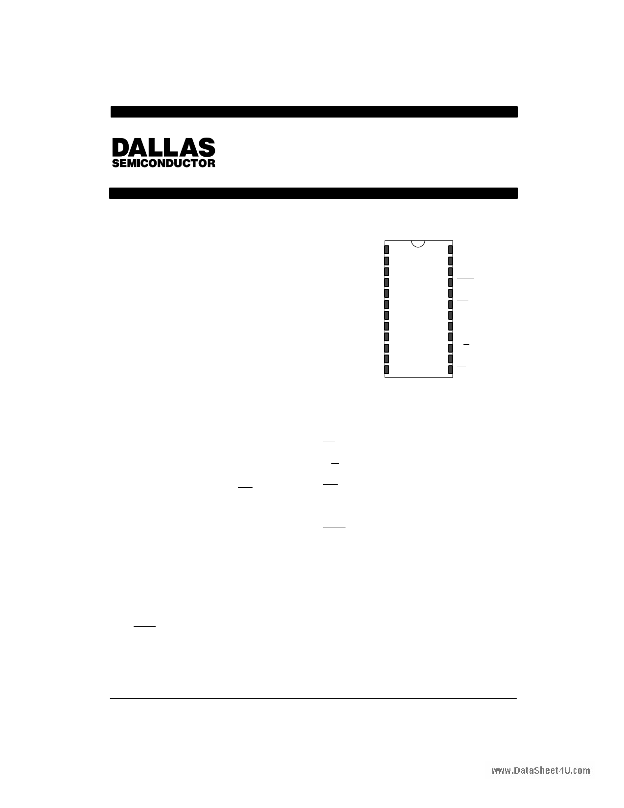
PIN ASSIGNMENT
NC
NC
NC
AD0
AD1
AD2
AD3
AD4
AD5
AD6
AD7
GND
1
2
3
4
5
6
7
8
9
10
11
12
24 VCC
23 SQW
22 NC
21 RCLR
20 NC
19 IRQ
18 NC
17 DS
16 NC
15 R/W
14 AS
13 CS
24 PIN ENCAPSULATED PACKAGE
PIN DESCRIPTION
AD0-AD7
NC
CS
AS
R/W
DS
IRQ
SQW
VCC
GND
RCLR
– Multiplexed Address/Data Bus
– No Connection
– Chip Select
– Address Strobe
– Read/Write Input
– Data Strobe
– Interrupt Request Output
– Square Wave Output
– +5 Volt Supply
– Ground
– RAM Clear
DESCRIPTION
The DS12B887 Real Time Clock plus RAM is designed
to be a direct replacement for the DS1287A or
DS12887A. The DS12B887 is identical in form, fit, and
function to the DS1287A or DS12887A, with the excep-
tion of RCLR, and has an additional 64 bytes of general
purpose RAM. Access to this additional RAM space is
determined by the logic level presented on AD6 during
the address portion of an access cycle. A lithium energy
source, quartz crystal, and write-protection circuitry are
contained within a 24-pin dual in-line package. As such,
the DS12B887 is a complete subsystem replacing 16
components in a typical application. The functions
include a nonvolatile time-of-day clock, an alarm, a one-
hundred-year calendar, programmable interrupt,
square wave generator, and 114 bytes of nonvolatile
static RAM. The real time clock is distinctive in that
time-of-day and memory are maintained even in the
absence of power.
ECopyright 1995 by Dallas Semiconductor Corporation.
All Rights Reserved. For important information regarding
patents and other intellectual property rights, please refer to
Dallas Semiconductor data books.
080895 1/16
1 page 
DS12B887
www.DataSheet4U.com
ADDRESS MAP DS12B887 Figure 2
0 00
14 BYTES
13 0D
14 0E
127 7F
0 SECONDS
1 SECONDS ALARM
2 MINUTES
3 MINUTES ALARM
4 HOURS
5 HOURS ALARM
6 DAY OF THE WEEK
7 DAY OF THE MONTH
8 MONTH
9 YEAR
10 REGISTER A
11 REGISTER B
12 REGISTER C
13 REGISTER D
TIME, CALENDAR AND ALARM LOCATIONS
The time and calendar information is obtained by read-
ing the appropriate memory bytes. The time, calendar,
and alarm are set or initialized by writing the appropriate
RAM bytes. The contents of the ten time, calendar, and
alarm bytes can be either Binary or Binary-Coded Deci-
mal (BCD) format. Before writing the internal time, cal-
endar, and alarm registers, the SET bit in Register B
should be written to a logic one to prevent updates from
occurring while access is being attempted. In addition
to writing the ten time, calendar, and alarm registers in a
selected format (binary or BCD), the data mode bit (DM)
of Register B must be set to the appropriate logic level.
All ten time, calendar, and alarm bytes must use the
same data mode. The set bit in Register B should be
cleared after the data mode bit has been written to allow
the real time clock to update the time and calendar
bytes. Once initialized, the real time clock makes all
updates in the selected mode. The data mode cannot
be changed without reinitializing the ten data bytes.
Table 2 shows the binary and BCD formats of the ten
time, calendar, and alarm locations. The 24-12 bit can-
not be changed without reinitializing the hour locations.
When the 12-hour format is selected, the high order bit
of the hours byte represents PM when it is a logic one.
The time, calendar, and alarm bytes are always acces-
sible because they are double buffered. Once per
second the ten bytes are advanced by one second and
checked for an alarm condition. If a read of the time and
calendar data occurs during an update, a problem exists
where seconds, minutes, hours, etc. may not correlate.
The probability of reading incorrect time and calendar
data is low. Several methods of avoiding any possible
incorrect time and calendar reads are covered later in
this text.
The three alarm bytes can be used in two ways. First,
when the alarm time is written in the appropriate hours,
minutes, and seconds alarm locations, the alarm inter-
rupt is initiated at the specified time each day if the alarm
enable bit is high . The second use condition is to insert
a “don’t care” state in one or more of the three alarm
bytes. The “don’t care” code is any hexadecimal value
from C0 to FF. The two most significant bits of each byte
set the “don’t care” condition when at logic 1. An alarm
will be generated each hour when the “don’t care” bits
are set in the hours byte. Similarly, an alarm is gener-
ated every minute with “don’t care” codes in the hours
and minute alarm bytes. The “don’t care” codes in all
three alarm bytes create an interrupt every second.
080895 5/16
5 Page 
DS12B887
www.DataSheet4U.com
ABSOLUTE MAXIMUM RATINGS*
Voltage on Any Pin Relative to Ground
Operating Temperature
Storage Temperature
Soldering Temperature
–0.3V to +7.0V
0°C to 70°C
–40°C to +70°C
260°C for 10 seconds
* This is a stress rating only and functional operation of the device at these or any other conditions above those
indicated in the operation sections of this specification is not implied. Exposure to absolute maximum rating
conditions for extended periods of time may affect reliability.
The Dallas Semiconductor DS12B887 built to the highest quality standards and manufactured for long term reliability.
All Dallas Semiconductor devices are made using the same quality materials and manufacturing methods. However,
standard versions of the DS12B887 are not exposed to environmental stresses, such as burn–in, that some industrial
applications require. For specific reliability information on this product, please contact the factory in Dallas at (214)
450–0448.
RECOMMENDED DC OPERATING CONDITIONS
PARAMETER
SYMBOL MIN
Power Supply Voltage
Input Logic 1
Input Logic 0
VCC 4.5
VIH 2.2
VIL -0.3
DC ELECTRICAL CHARACTERISTICS
PARAMETER
SYMBOL
Power Supply Current
Input Leakage
I/O Leakage
Output @ 2.4V
Output @ 0.4V
Write Protect Voltage
ICC1
IIL
ILO
IOH
IOL
VTP
MIN
-1.0
-1.0
-1.0
4.0
CAPACITANCE
PARAMETER
Input Capacitance
Output Capacitance
SYMBOL
CIN
COUT
MIN
(0°C to 70°C)
TYP
MAX
UNITS NOTES
5.0 5.5 V
1
VCC+0.3
+0.8
V
V
1
1
(0°C to 70°C; VCC = 4.5 to 5.5V)
TYP
MAX
UNITS NOTES
7 15 mA 2
+1.0 mA
+1.0 mA
3
mA 1,4
4.0 mA
1
4.25 4.5
V
(tA = 25°C)
TYP
MAX
UNITS NOTES
5 pF
7 pF
080895 11/16
11 Page | ||
| Páginas | Total 16 Páginas | |
| PDF Descargar | [ Datasheet DS12B887.PDF ] | |
Hoja de datos destacado
| Número de pieza | Descripción | Fabricantes |
| DS12B887 | Real Time Clock | Dallas Semiconductor |
| Número de pieza | Descripción | Fabricantes |
| SLA6805M | High Voltage 3 phase Motor Driver IC. |
Sanken |
| SDC1742 | 12- and 14-Bit Hybrid Synchro / Resolver-to-Digital Converters. |
Analog Devices |
|
DataSheet.es es una pagina web que funciona como un repositorio de manuales o hoja de datos de muchos de los productos más populares, |
| DataSheet.es | 2020 | Privacy Policy | Contacto | Buscar |