|
|
|
PDF ADS5421 Data sheet ( Hoja de datos )
| Número de pieza | ADS5421 | |
| Descripción | 40MHz Sampling ANALOG-TO-DIGITAL CONVERTER | |
| Fabricantes | Burr-Brown Corporation | |
| Logotipo | ||
Hay una vista previa y un enlace de descarga de ADS5421 (archivo pdf) en la parte inferior de esta página. Total 21 Páginas | ||
|
No Preview Available !
ADS5421
ADS5421
SBAS237D – DECEMBER 2001 – REVISED JULY 2004
14-Bit, 40MHz Sampling
ANALOG-TO-DIGITAL CONVERTER
FEATURES
q HIGH DYNAMIC RANGE:
High SFDR: 83dB at 10MHz fIN
www.DataSheet4U.com High SNR: 75dB at 10MHz f
IN
q PREMIUM TRACK-AND-HOLD:
Differential Inputs
Selectable Full-Scale Input Range
q LOW POWER: 850mW
q FLEXIBLE CLOCKING:
Differential or Single-Ended
Accepts Sine or Square Wave Clocking Down to
0.5Vp-p
Variable Threshold Level
APPLICATIONS
q COMMUNICATIONS RECEIVERS
q TEST INSTRUMENTATION
q PROFESSIONAL CCD IMAGING
DESCRIPTION
The ADS5421 is a high-dynamic range 14-bit, 40MHz,
pipelined Analog-to-Digital Converter (ADC). It includes a
high-bandwidth linear track-and-hold amplifier that gives
excellent spurious performance up to and beyond the Nyquist
rate. The clock input can accept a low-level differential sine
wave or square wave signal down to 0.5Vp-p, further improving
the Signal-to-Noise Ratio (SNR) performance.
The ADS5421 has a 4Vp-p differential input range
(2Vp-p • 2 inputs) for optimum Spurious-Free Dynamic
Range (SFDR). The differential operation gives the lowest
even-order harmonic components. A lower input voltage can
also be selected using the internal references, further
optimizing SFDR.
The ADS5421 is available in a small LQFP-64 package.
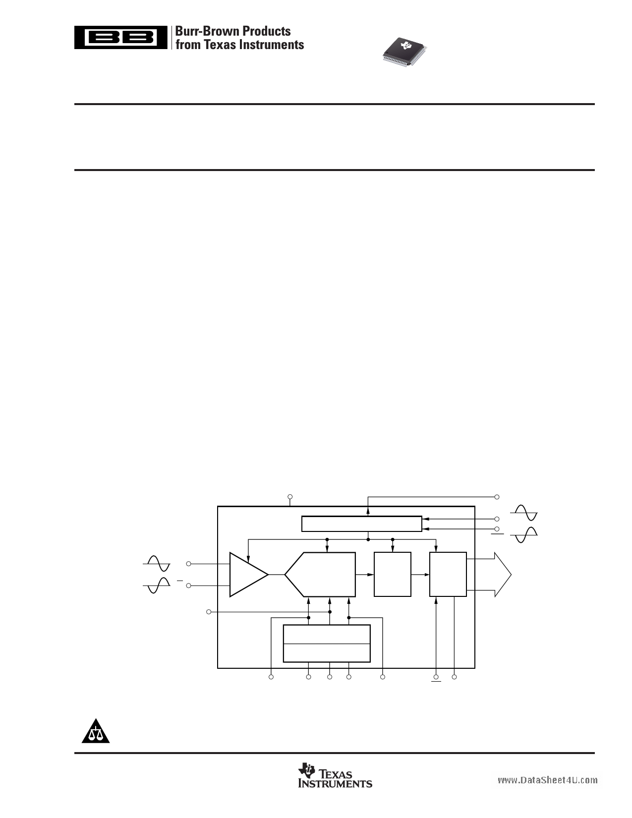
1Vp-p
1Vp-p
ADS5421
IN
IN
CM
(+2.5V)
T&H
+VS
Timing Circuitry
14-Bit
Pipelined
ADC
Core
Error
Correction
Logic
DV
CLK
CLK
3-State
Outputs
D0
•••
D13
Reference Ladder
and Driver
Reference and
Mode Select
REFT
VREF SEL1 SEL2 REFB
OE VDRV
Please be aware that an important notice concerning availability, standard warranty, and use in critical applications of
Texas Instruments semiconductor products and disclaimers thereto appears at the end of this data sheet.
PRODUCTION DATA information is current as of publication date.
Products conform to specifications per the terms of Texas Instruments
standard warranty. Production processing does not necessarily include
testing of all parameters.
www.ti.com
Copyright © 2001-2004 Texas Instruments, Incorporated
1 page 
TIMING DIAGRAM
Analog In N
Clock
N+1
N+2
tD tCONV
N+3
N+4
tL tH
N+5
N+6
N+7
N+8
N+9
N + 10
Data Out
Data Valid Output
www.DataSheet4U.com
tDV
N – 10 N – 9
Data Invalid
N–8
10 Clock Cycles
N–7
N–6
N–5
N–4
N–3
N–2
N–1
t2
N
t1
SYMBOL
DESCRIPTION
t CONV
tL
tH
tD
t1
t2
tDV
Convert Clock Period
Clock Pulse LOW
Clock Pulse HIGH
Aperture Delay
Data Hold Time, CL = 0pF
New Data Delay Time, CL = 15pF max
Data Valid Output, CL = 15pF
MIN
25
11.5
11.5
3.9
TYP
t CONV / 2
t CONV / 2
3
7.2
12.7
4.4
MAX
1µs
UNITS
ns
ns
ns
ns
ns
ns
ns
REFERENCE AND FULL-SCALE RANGE SELECT TABLE
DESIRED FULL-SCALE RANGE
4Vp-p
3Vp-p
2Vp-p
SEL1
GND
GND
VREF
SEL2
GND
+VSA
GND
INTERNAL VREF
2V
1.5V
1V
NOTE: For external reference operation, tie VREF to +VSA. The full-scale range will be 2x the reference value. For example, selecting a 2V external reference
will set the full-scale values of 1.5V to 3.5V for both IN and IN inputs.
ADS5421
SBAS237D
www.ti.com
5
5 Page 
VIN (IF)
Optional
Bandpass
Filter
IF
Amplifier
RS
XFR
1:n
RIN
RT RIN
NOTE: Supply bypassing not shown.
+5V
IN
CIN ADS5421
IN
CM
+
2.2µF
0.1µF
www.DataSheet4U.cFoImGURE 4. Driving the ADS5421 with a Low-Distortion IF Amplifier and a Transformer Suited for IF Sampling Applications.
TRANSFORMER-COUPLED, SINGLE-ENDED-TO-
DIFFERENTIAL CONFIGURATION
For applications in which the input frequency is limited to
approximately 10MHz (e.g., baseband), a high-speed opera-
tional amplifier may be used. The OPA847 is configured for the
noninverting mode; this amplifies the single-ended input signal
and drives the primary of a RF transformer (see Figure 5). To
maintain the very low distortion performance of the OPA847, it
may be advantageous to set the full-scale input range of the
ADS5421 to 3Vp-p or 2Vp-p (refer to the Reference section for
details on selecting the converter’s full-scale range).
The circuit also shows the use of an additional RC low-pass
filter placed in series with each converter input. This optional
filter can be used to set a defined corner frequency and
attenuate some of the wideband noise. The actual compo-
nent values would need to be tuned for individual application
requirements. As a guideline, resistor values are typically in
the range of 10Ω to 50Ω, and capacitors in the range of 10pF
to 100pF. In any case, the RIN and CIN values should have
a low tolerance. This will ensure that the ADS5421 sees
closely matched source impedances.
+5V –5V
VIN
OPA847
R1
R2
RG
RS 0.1µF
1:n
RIN
RT RIN
+5V
IN
CIN
IN
VCM ≈ +2.5V
ADS5421
CM
+
2.2µF
0.1µF
FIGURE 5. Converting a Single-Ended Input Signal into a Differential Signal Using a RF Transformer.
ADS5421
SBAS237D
www.ti.com
11
11 Page | ||
| Páginas | Total 21 Páginas | |
| PDF Descargar | [ Datasheet ADS5421.PDF ] | |
Hoja de datos destacado
| Número de pieza | Descripción | Fabricantes |
| ADS5421 | 40MHz Sampling ANALOG-TO-DIGITAL CONVERTER | Burr-Brown Corporation |
| ADS5421 | 14-Bit 40MHz Sampling Analog-to-Digital Converter (Rev. E) | Texas Instruments |
| ADS5422 | 14-Bit 62MSPS Sampling Analog-To-Digital Converter (Rev. D) | Texas Instruments |
| ADS5423 | ADS5423: 14-Bit 80 MSPS ADC (Rev. A) | Texas Instruments |
| Número de pieza | Descripción | Fabricantes |
| SLA6805M | High Voltage 3 phase Motor Driver IC. |
Sanken |
| SDC1742 | 12- and 14-Bit Hybrid Synchro / Resolver-to-Digital Converters. |
Analog Devices |
|
DataSheet.es es una pagina web que funciona como un repositorio de manuales o hoja de datos de muchos de los productos más populares, |
| DataSheet.es | 2020 | Privacy Policy | Contacto | Buscar |