|
|
|
PDF DS32ELX0124 Data sheet ( Hoja de datos )
| Número de pieza | DS32ELX0124 | |
| Descripción | Deserializer | |
| Fabricantes | National Semiconductor | |
| Logotipo | ||
Hay una vista previa y un enlace de descarga de DS32ELX0124 (archivo pdf) en la parte inferior de esta página. Total 24 Páginas | ||
|
No Preview Available !
PRELIMINARY
May 9, 2008
DS32EL0124 DS32ELX0124
125 MHz — 312.5 MHz Deserializer with DDR LVDS Parallel
Interface
General Description
The DS32EL0124/DS32ELX0124 integrates clock and data
recovery modules for high-speed serial communication over
FR-4 printed circuit board backplanes, balanced cables, and
optical fiber. This easy-to-use chipset integrates advanced
signal and clock conditioning functions, with an FPGA friendly
www.DataSheeitn4tUer.cfaocme.
The DS32EL0124/DS32ELX0124 deserializes up to 3.125
Gbps of high speed serial data to 5 LVDS outputs without the
need for an external reference clock. With DC-balance de-
coding enabled, the application payload of 2.5 Gbps is dese-
rialized to 4 LVDS outputs.
The DS32EL0124/DS32ELX01214 deserializers feature a re-
mote sense capability to automatically signal link status con-
ditions to its companion DS32EL0421/ELX0421 serializers
without requiring an additional feedback path.
The parallel LVDS interface of these devices reduce FPGA
I/O pins, board trace count and alleviates EMI issues, when
compared to traditional single-ended wide bus interfaces.
The DS32EL0124/ELX0124 is programmable through a SM-
Bus interface as well as through control pins.
Applications
■ Imaging: Industrial, Medical Security, Printers
■ Displays: LED walls, Commercial
■ Video Transport
■ Communication Systems
■ Test and Measurement
■ Industrial Bus
Features
■ 5-bit LVDS parallel data interface
■ Programmable Receive Equalization
■ Selectable DC-balance decoder
■ Selectable De-scrambler
■ Remote Sense for automatic detection and negotiation of
link status
■ No external receiver reference clock required
■ LVDS parallel interface
■ Programmable LVDS output clock delay
■ Supports output data-valid signaling
■ Supports keep-alive clock output
■ On chip LC VCOs
■ Redundant serial input (ELX device only)
■ Retimed serial output (ELX device only)
■ Configurable PLL loop bandwidth
■ Configurable via SMBus
■ Loss of lock and error reporting
■ 48-pin LLP package with exposed DAP
Key Specifications
■ 1.25 to 3.125 Gbps serial data rate
■ 125 to 312.5 MHz DDR parallel clock
■ -40° to +85°C temperature range
■ > 8 kV ESD (HBM) protection
■ High Jitter Tolerance TBD
■ Low Jitter Transfer TBD
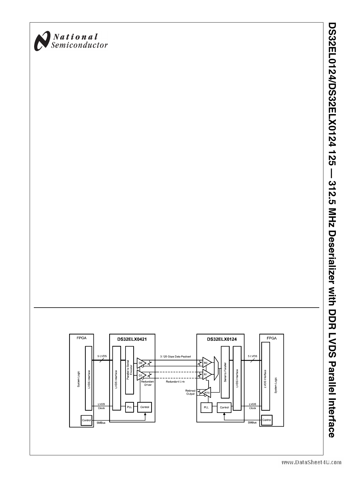
Typical Application
© 2008 National Semiconductor Corporation 300431
30043101
www.national.com
1 page 
NC
2 ,8, 9, 10, 12, 13, 14, 19, Misc.
No Connect, for DS32EL0124
20, 21, 22, 23, 24, 29
8, 9, 10, 13, 23, 24, 29 Misc
No Connect, for DS32ELX0124
www.DataSheet4U.com
5 www.national.com
5 Page 
Functional Description
POWER SUPPLIES
The DS32EL0124 and DS32ELX0124 have several power
supply pins, at 2.5V as well as 3.3V. It is important that these
pins all be connected and properly bypassed. Bypassing
should consist of parallel 4.7μF and 0.1μF capacitors as a
minimum, with a 0.1μF capacitor on each power pin. A 22 μF
capacitor is required on the VDDPLL pin which is connected
to the 3.3V rail.
These devices have a large contact in the center on the bot-
tom of the package. This contact must be connected to the
system GND as it is the major ground connection for the de-
vice.
POWER UP
It is recommended, although not necessary, to bring up the
www.Data3S.h3eVept4oUw.ecor msupply before the 2.5V supply. If the 2.5V supply
is powered up first, an initial current draw of approximately
600mA from the 2.5V rail may occur before settling to its final
value. Regardless of the sequence, both power rails should
monotonically ramp up to their final values.
POWER MANAGEMENT
These devices have two methods to reduce power consump-
tion. To enter the first power save mode, the on board host
FPGA or controlling device can cease to output the DDR
transmit clock. To further reduce power, a write to the power
down register will put the device in its lowest power mode.
RESET
There are three ways to reset these devices. A reset occurs
automatically during power-up. The device can also be reset
by pulling the RESET pin low, with normal operation resuming
when the pin is driven high again. The device can also be
reset by writing to the reset register. This reset will put all of
the register values back to their default values, except it will
not affect the address register value if the SMBus default ad-
dress has been changed.
LVDS OUTPUTS
The DS32EL0124 and DS32ELX0124 has standard LVDS
outputs, compatible with ANSI/TIA/EIA-644. It is recommend-
ed that the PCB trace between the FPGA and the deserializer
output be no more than 40-inches. Longer PCB traces may
introduce signal degradation as well as channel skew which
could cause serialization errors. The connection between the
host and the DS32EL0124 or DS32ELX0124 should be over
a controlled impedance transmission line with impedance that
matches the termination resistor – usually 100Ω. Setup and
hold times are specified in the LVDS Switching Characteris-
tics table, however the clock delay can be adjusted by writing
to register 30’h.
LOOP FILTER
The DS32EL0124 and DSELX0124 have an internal clock
data recovery module (CDR), which is used to recover the
input serial data. The loop filter for this CDR is external, and
for optimum results, a 30nF capacitor should be connected
between pins 26 and 27. See the Typical Interface Circuit
(Figure 11).
REMOTE SENSE
The remote sense feature can be used when a DS32EL0421
or DS32ELX0421 serializer is directly connected to a
DS32EL0124 or DS32ELX0124 deserializer. Active compo-
nents in the signal path between the serializer and the dese-
rializer may interfere with the back channel signaling of the
devices.
When remote sense is enabled, the deserializer will cycle
through five states to successfully establish a link and align
the data. The state diagram for the deserialiezr is shown in
Figure 7. The deserialzer will remain in the low power IDLE
state until it receives an input signal. Once the CDR of the
deserializer has locked to the input clock, the device will enter
the LINK DETECT state. While in this state, the serializer will
monitor the line to see if the deserializer is present. If a de-
serializer is detected the serializer will enter the LINK AC-
QUISITION state. The serializer will transmit the entire
training pattern and then enter the NORMAL state. If the de-
serializer is unable to successfully lock or maintain lock, it will
break the link sending the serializer back to the IDLE or LINK
DETECT states.
DC-BALANCE DECODER
The DS32EL0124 and DS32ELX0124 have a built-in DC-bal-
ance decoder to support AC-coupled applications. When en-
abled, the output signal RxOUT4+/-, is treated as a data valid
bit. If RxOUT+/- is low, then the data output from RxOUT0-
RxOUT3 has been successfully decoded using the 8b/10b
coding scheme. If RxOUT4+/- is high and the outputs Rx-
OUT0 -RxOUT3 are high then an invalid 8b/10b code was
received, signifying a bit error. If RxOUT4+/- is high and the
outputs RxOUT0 -RxOUT3 are low then an idle character has
been received. The default idle character is a K28.5 code. In
order to properly receive other Kcodes, they must first be pro-
grammed into the deserializer via the SMBus.
11 www.national.com
11 Page | ||
| Páginas | Total 24 Páginas | |
| PDF Descargar | [ Datasheet DS32ELX0124.PDF ] | |
Hoja de datos destacado
| Número de pieza | Descripción | Fabricantes |
| DS32ELX0124 | DS32EL0124/ELX0124 125MHz-312.5MHz FPGA-Link Deserializr w/DDR LVDS Para I/F (Rev. K) | Texas Instruments |
| DS32ELX0124 | Deserializer | National Semiconductor |
| Número de pieza | Descripción | Fabricantes |
| SLA6805M | High Voltage 3 phase Motor Driver IC. |
Sanken |
| SDC1742 | 12- and 14-Bit Hybrid Synchro / Resolver-to-Digital Converters. |
Analog Devices |
|
DataSheet.es es una pagina web que funciona como un repositorio de manuales o hoja de datos de muchos de los productos más populares, |
| DataSheet.es | 2020 | Privacy Policy | Contacto | Buscar |