|
|
|
PDF GSC24BC04 Data sheet ( Hoja de datos )
| Número de pieza | GSC24BC04 | |
| Descripción | (GSC24BC01 - GSC24BC16) 2-WIRE SERIAL EEPROMS | |
| Fabricantes | GTM | |
| Logotipo | ||
Hay una vista previa y un enlace de descarga de GSC24BC04 (archivo pdf) en la parte inferior de esta página. Total 9 Páginas | ||
|
No Preview Available !
www.DataSheet4U.com
ISSUED DATE :2006/06/14
REVISED DATE :
GSC24BC01/02/04/08/16
2-wire Serial EEPROMs 1K/2K/4K/8K/16K
Description
The GSC24BC family provides 1K, 2K, 4K, 8K and 16K of serial electrically erasable and programmable
read-only memory (EEPROM). The wide Vdd range allows for low-voltage operation down to 1.8V. The device,
fabricated using traditional CMOS EEPROM technology, is optimized for many industrial and commercial
applications where low-voltage and low-power operation is essential. The device is accessed via a 2-wire serial
interface.
Features
Internally organized as 128x8 (1K), 256x8 (2K)
512x8 (4K), 1024x8 (8K), 2048x8 (16K),
Low-voltage and standard-voltage operation:
1.8V~5.5V
-wire serial interface bus
Date retention: 100years
High endurance: 1,000,000 Write Cycles
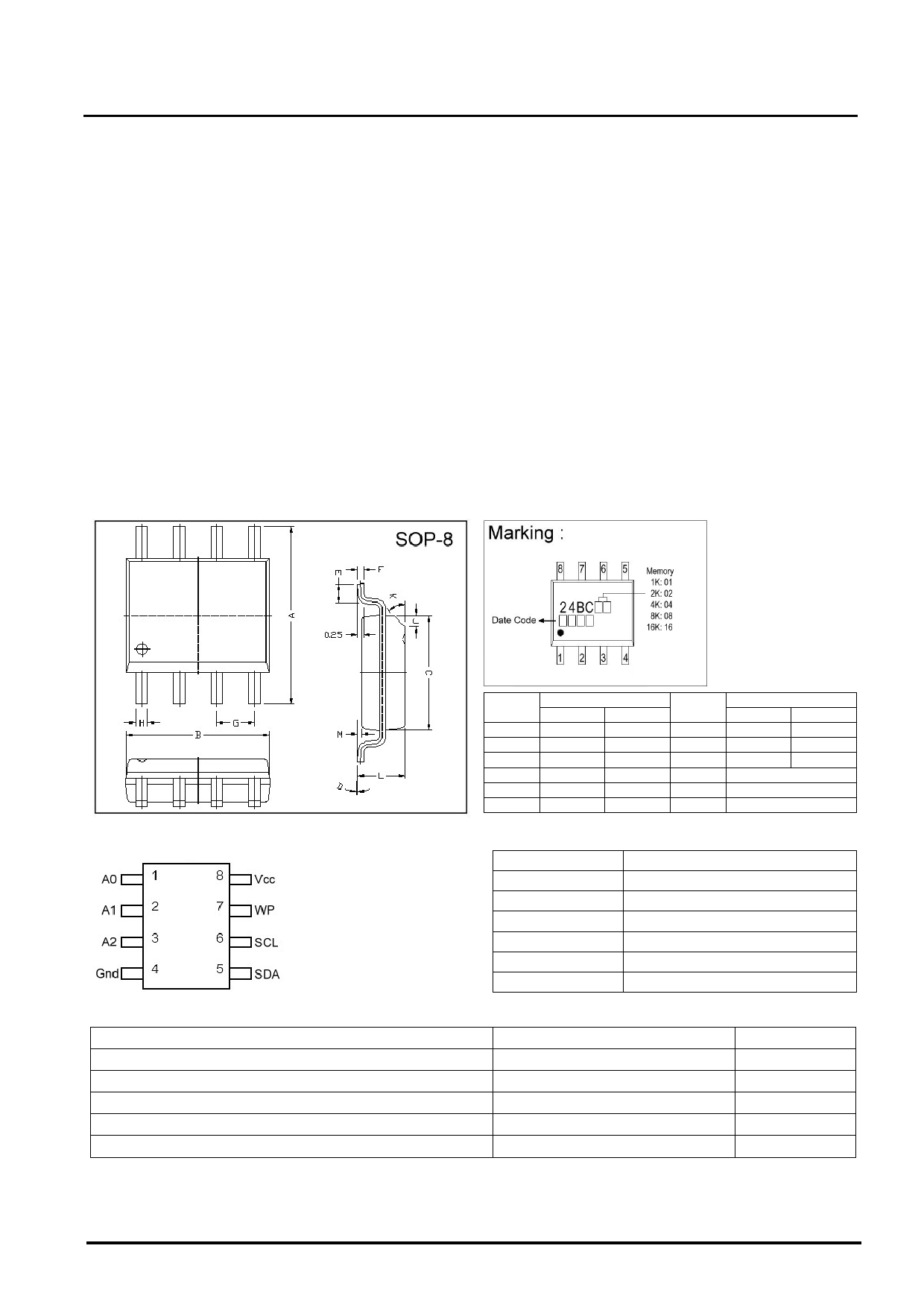
Package Dimensions
100KHz (1.8V) & 400KHz (5V) compatibility
Bi-directional data transfer protocol
Self-timed write cycle (5ms max)
Write protect pin for hardware data protection
8-byte page (1K, 2K) and 16-byte page (4K,8K,16K)
write modes
Allows for partial page write
REF.
A
B
C
D
E
F
Millimeter
Min. Max.
5.80
6.20
4.80
5.00
3.80
4.00
0° 8°
0.40
0.90
0.19
0.25
REF.
M
H
L
J
K
G
Millimeter
Min. Max.
0.10
0.25
0.35
0.49
1.35
1.75
0.375 REF.
45°
1.27 TYP.
Figure 1. Pin Configurations
Pin Name
A0 – A2
SDA
SCL
WP
Gnd
Vcc
Function
Address inputs
Serial Data
Serial Clock Input
Write Protect
Ground
Power Supply
Absolute Maximum Ratings
Parameter
Ratings
Unit
Voltage on Any Pin with Respect to Ground
-0.8 to Vcc +1.5
V
Maximum Operating Voltage
6.25 V
DC Output Current
5.0 mA
Operating Temperature Range
-55 ~ +125
Storage Temperature Range
-65 ~ +150
Note: Stresses beyond those listed under “Absolute Maximum Ratings” may cause permanent damage to the device. This is a stress
rating only and functional operation of the device at these or any other conditions beyond those indicated in the operational sections of
these specifications are not implied. Exposure to absolute maximum rating conditions for extended periods may affect device reliability.
GSC24BC01/02/02/04/08/16
Page: 1/9
1 page 
BUS TIMING
Figure 3. SCL: Serial Clock, SDA: Serial Data I/O
ISSUED DATE :2006/06/14
REVISED DATE :
WRITE CYCLE TIMING
Figure 4. SCL: Serial Clock, SDA: Serial Data I/O
Note: 1. The write cycle time tWR is the time from a valid stop condition of a write sequence to the end of the internal
clear/write cycle
Figure 5. DATA VALIDITY
GSC24BC01/02/02/04/08/16
Page: 5/9
5 Page | ||
| Páginas | Total 9 Páginas | |
| PDF Descargar | [ Datasheet GSC24BC04.PDF ] | |
Hoja de datos destacado
| Número de pieza | Descripción | Fabricantes |
| GSC24BC01 | (GSC24BC01 - GSC24BC16) 2-WIRE SERIAL EEPROMS | GTM |
| GSC24BC02 | (GSC24BC01 - GSC24BC16) 2-WIRE SERIAL EEPROMS | GTM |
| GSC24BC04 | (GSC24BC01 - GSC24BC16) 2-WIRE SERIAL EEPROMS | GTM |
| GSC24BC08 | (GSC24BC01 - GSC24BC16) 2-WIRE SERIAL EEPROMS | GTM |
| Número de pieza | Descripción | Fabricantes |
| SLA6805M | High Voltage 3 phase Motor Driver IC. |
Sanken |
| SDC1742 | 12- and 14-Bit Hybrid Synchro / Resolver-to-Digital Converters. |
Analog Devices |
|
DataSheet.es es una pagina web que funciona como un repositorio de manuales o hoja de datos de muchos de los productos más populares, |
| DataSheet.es | 2020 | Privacy Policy | Contacto | Buscar |