|
|
|
PDF DS26303 Data sheet ( Hoja de datos )
| Número de pieza | DS26303 | |
| Descripción | Octal Line Interface Unit | |
| Fabricantes | Maxim Integrated Products | |
| Logotipo | ||
Hay una vista previa y un enlace de descarga de DS26303 (archivo pdf) en la parte inferior de esta página. Total 70 Páginas | ||
|
No Preview Available !
www.DataSheet4U.com
www.maxim-ic.com
GENERAL DESCRIPTION
The DS26303 is an 8-channel short-haul line
interface unit (LIU) that supports E1/T1/J1 from a
single 3.3V power supply. A wide variety of
applications are supported through internal
termination or external termination. A single bill of
material can support E1/T1/J1 with minimum external
components. Redundancy is supported through
nonintrusive monitoring, optimal high-impedance
modes, and configurable 1:1 or 1+1 backup
enhancements. An on-chip synthesizer generates the
E1/T1/J1 clock rates by a single master clock input of
various frequencies. Two clock output references are
also offered.
APPLICATIONS
T1 Digital Cross-Connects
ATM and Frame Relay Equipment
Wireless Base Stations
ISDN Primary Rate Interface
E1/T1/J1 Multiplexer and Channel Banks
E1/T1/J1 LAN/WAN Routers
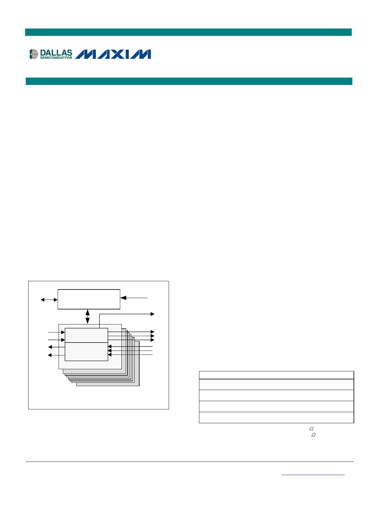
FUNCTIONAL DIAGRAM
Jtag
RTIP
RRING
TTTIP
TRING
Software Control,
Hardware Control
and JTAG
MODESEL
RLOS
Receiver
Transmitter
1
RPOS
RNEG
RCLK
TPOS
TNEG
TCLK
8
DS26303
DS26303
3.3V, E1/T1/J1, Short-Haul,
Octal Line Interface Unit
FEATURES
8 Complete E1, T1, or J1 Short-Haul Line
Interface Units
Independent E1, T1, or J1 Selections
Internal Software-Selectable Transmit and
Receive-Side Termination
Crystal-Less Jitter Attenuator
Selectable Single-Rail and Dual-Rail Mode
and AMI or HDB3/B8ZS Line Encoding and
Decoding
Detection and Generation of AIS
Digital/Analog Loss-of-Signal Detection as
per T1.231, G.775, and ETS 300 233
External Master Clock can be Multiple of
2.048MHz or 1.544MHz for T1/J1 or E1
Operation; This Clock will be Internally
Adapted for T1 or E1 Use
Built-In BERT Tester for Diagnostics
8-Bit Parallel Interface Support for Intel or
Motorola Mode or a 4-Wire Serial Interface
Hardware Mode Interface Support
Transmit Short-Circuit Protection
G.772 Nonintrusive Monitoring
Specification Compliance to the Latest T1
and E1 Standards—ANSI T1.102, AT&T Pub
62411, T1.231, T1.403, ITU-T G.703, G.742,
G.775, G.823, ETS 300 166, and ETS 300 233
Single 3.3V Supply with 5V Tolerant I/O
JTAG Boundary Scan as per IEEE 1149.1
144-Pin eLQFP Package
ORDERING INFORMATION
PART
DS26303L-XXX
TEMP RANGE PIN-PACKAGE
0°C to +70°C 144 eLQFP
DS26303L-XXX+
0°C to +70°C 144 eLQFP
DS26303LN-XXX -40°C to +85°C 144 eLQFP
DS26303LN-XXX+ -40°C to +85°C 144 eLQFP
Note: When XXX is 075, the part defaults to 75Ω impedance in E1
mode; when XXX is 120, the part defaults to 120Ω impedance.
+ Denotes a lead-free/RoHS-compliant package.
e = Exposed Pad.
Note: Some revisions of this device may incorporate deviations from published specifications known as errata. Multiple revisions of any device
may be simultaneously available through various sales channels. For information about device errata, click here: www.maxim-ic.com/errata.
1 of 101
REV: 053107
1 page 
DS26303: 3.3V, T1/E1/J1, Short-Haul, Octal Line Interface Unit
LIST OF TABLES
Table 2-1. T1-Related Telecommunications Specifications ........................................................................................ 7
Table 2-2. E1-Related Telecommunications Specifications ........................................................................................ 8
Table 4-1. Pin Descriptions........................................................................................................................................ 11
Table 4-2. Hardware Mode Configuration Examples................................................................................................. 20
Table 4-3. Parallel Port Mode Selection and Pin Functions ...................................................................................... 22
Table 5-1. Primary Register Set ................................................................................................................................ 24
Table 5-2. Secondary Register Set............................................................................................................................ 25
Table 5-3. Individual LIU Register Set....................................................................................................................... 25
Table 5-4. BERT Register Set ................................................................................................................................... 26
Table 5-5. Primary Register Set Bit Map ................................................................................................................... 27
Table 5-6. Secondary Register Set Bit Map .............................................................................................................. 27
Table 5-7. Individual LIU Register Set Bit Map.......................................................................................................... 28
Table 5-8. BERT Register Bit Map ............................................................................................................................ 28
Table 5-9. G.772 Monitoring Control ......................................................................................................................... 32
Table 5-10. TST Template Select Transceiver Register ........................................................................................... 35
Table 5-11. Template Selection................................................................................................................................. 35
Table 5-12. Address Pointer for Bank Selection........................................................................................................ 37
Table 5-13. MCLK Selections .................................................................................................................................... 42
Table 5-14. Jitter Attenuator Bandwidth Selections................................................................................................... 43
Table 5-15. PLL Clock Select .................................................................................................................................... 45
Table 5-16. Clock A Select ........................................................................................................................................ 45
Table 6-1. Telecommunications Specification Compliance for DS26303 Transmitters ............................................ 55
Table 6-2. Registers Related to Control of DS26303 Transmitters ........................................................................... 55
Table 6-3. DS26303 Template Selections................................................................................................................. 56
Table 6-4. LIU Front-End Values ............................................................................................................................... 58
Table 6-5. Loss Criteria T1.231, G.775, and ETS 300 233 Specifications................................................................ 60
Table 6-6. AIS Criteria T1.231, G.775, and ETS 300 233 Specifications.................................................................. 61
Table 6-7. AIS Detection and Reset Criteria ............................................................................................................. 61
Table 6-8. Registers Related to AIS Detection.......................................................................................................... 61
Table 6-9. BPV, Code Violation, and Excessive Zero Error Reporting ..................................................................... 62
Table 6-10. Pseudorandom Pattern Generation........................................................................................................ 68
Table 6-11. Repetitive Pattern Generation ................................................................................................................ 68
Table 7-1. Instruction Codes for IEEE 1149.1 Architecture....................................................................................... 76
Table 7-2. ID Code Structure..................................................................................................................................... 77
Table 7-3 Device ID Codes........................................................................................................................................ 77
Table 8-1. Recommended DC Operating Conditions ................................................................................................ 78
Table 8-2. Capacitance.............................................................................................................................................. 78
Table 8-3. DC Characteristics.................................................................................................................................... 78
Table 9-1. Thermal Characteristics............................................................................................................................ 79
Table 10-1. Transmitter Characteristics..................................................................................................................... 80
Table 10-2. Receiver Characteristics......................................................................................................................... 80
Table 10-3. Intel Read Mode Characteristics ............................................................................................................ 81
Table 10-4. Intel Write Cycle Characteristics ............................................................................................................ 84
Table 10-5. Motorola Read Cycle Characteristics ..................................................................................................... 87
Table 10-6. Motorola Write Cycle Characteristics ..................................................................................................... 90
Table 10-7. Serial Port Timing Characteristics .......................................................................................................... 93
Table 10-8. Transmitter System Timing .................................................................................................................... 94
Table 10-9. Receiver System Timing......................................................................................................................... 95
Table 10-10. JTAG Timing Characteristics................................................................................................................ 96
5 of 101
5 Page 
DS26303: 3.3V, T1/E1/J1, Short-Haul, Octal Line Interface Unit
4 PIN DESCRIPTION
Table 4-1. Pin Descriptions
NAME
PIN
TTIP1
TTIP2
TTIP3
TTIP4
TTIP5
TTIP6
TTIP7
TTIP8
TRING1
TRING2
TRING3
TRING4
TRING5
TRING6
TRING7
TRING8
RTIP1
RTIP2
RTIP3
RTIP4
RTIP5
RTIP6
RTIP7
RTIP8
RRING1
RRING2
RRING3
RRING4
RRING5
RRING6
RRING7
RRING8
45
52
57
64
117
124
129
136
46
51
58
63
118
123
130
135
48
55
60
67
120
127
132
139
49
54
61
66
121
126
133
138
TYPE
FUNCTION
ANALOG TRANSMIT AND RECEIVE
Analog
Output
Transmit Bipolar Tip for Channel 1 to 8. These pins are
differential line-driver tip outputs. These pins will be high
impedance if pin OE is low or the corresponding OEB.OEBn bit is
high. If the corresponding clock TCLKn is low for 64 MCLKs, the
corresponding transmitter is put in power-down mode. The
differential outputs of TTIPn and TRINGn can provide internal
matched impedance for E1 75Ω, E1 120Ω, T1 100Ω, or J1 110Ω.
Analog
Output
Transmit Bipolar Ring for Channel 1 to 8. These pins are
differential line-driver ring outputs. These pins will be high
impedance if pin OE is low or the corresponding OEB.OEBn bit is
high. If the corresponding clock TCLKn is low for 64 MCLKs, the
corresponding transmitter is put in power-down mode. The
differential outputs of TTIPn and TRINGn can provide internal
matched impedance for E1 75Ω, E1 120Ω, T1 100Ω, or J1 110Ω.
Analog
Input
Receive Bipolar Tip for Channel 1 to 8. Receive analog input for
differential receiver. Data and clock are recovered and output at
RPOSn/RNEGn and RCLKn pins, respectively. The differential
inputs of RTIPn and RRINGn can provide internal matched
impedance for E1 75Ω, E1 120Ω, T1 100Ω, or J1 110Ω.
Analog
Input
Receive Bipolar Ring for Channel 1 to 8. Receive analog input
for differential receiver. Data and clock are recovered and output
at RPOSn/RNEGn and RCLKn pins, respectively. The differential
inputs of RTIPn and RRINGn can provide internal matched
impedance for E1 75Ω, E1 120Ω, T1 100Ω, or J1 110Ω.
11 of 101
11 Page | ||
| Páginas | Total 70 Páginas | |
| PDF Descargar | [ Datasheet DS26303.PDF ] | |
Hoja de datos destacado
| Número de pieza | Descripción | Fabricantes |
| DS26303 | Octal Line Interface Unit | Maxim Integrated Products |
| Número de pieza | Descripción | Fabricantes |
| SLA6805M | High Voltage 3 phase Motor Driver IC. |
Sanken |
| SDC1742 | 12- and 14-Bit Hybrid Synchro / Resolver-to-Digital Converters. |
Analog Devices |
|
DataSheet.es es una pagina web que funciona como un repositorio de manuales o hoja de datos de muchos de los productos más populares, |
| DataSheet.es | 2020 | Privacy Policy | Contacto | Buscar |