|
|
PDF RF3807 Data sheet ( Hoja de datos )
| Número de pieza | RF3807 | |
| Descripción | GaAs HBT PRE-DRIVER AMPLIFIER | |
| Fabricantes | RF Micro Devices | |
| Logotipo |  |
|
Hay una vista previa y un enlace de descarga de RF3807 (archivo pdf) en la parte inferior de esta página. Total 18 Páginas | ||
|
No Preview Available !
www.DataSheet4U.com
RF3807
0 GaAs HBT PRE-DRIVER AMPLIFIER
RoHS Compliant & Pb-Free Product
Typical Applications
• GaAs Pre-Driver for Basestation Amplifiers
• Class AB Operation for NMT, GSM, DCS, PCS,
• PA Stage for Commercial Wireless Infrastructure UMTS, and WLAN Transceiver Applications
Product Description
The RF3807 is a GaAs pre-driver power amplifier, specifi-
cally designed for wireless infrastructure applications.
Using a highly reliable GaAs HBT fabrication process,
this high-performance single-stage amplifier achieves
high output power over a broad frequency range. The
RF3807 also provides excellent efficiency and thermal
stability through the use of a thermally-enhanced surface-
mount plastic-slug package. Ease of integration is accom-
plished through the incorporation of an optimized evalua-
tion board design provided to achieve proper 50Ω
operation. Various evaluation boards are available to
address a broad range of wireless infrastructure applica-
tions: NMT 450MHz; GSM850; GSM900; DCS1800;
PCS1900; UMTS2100; and, WLAN2400.
Optimum Technology Matching® Applied
Si BJT
9GaAs HBT
GaAs MESFET
Si Bi-CMOS
SiGe HBT
Si CMOS
InGaP/HBT
GaN HEMT
SiGe Bi-CMOS
VREF 1
NC 2
RFIN 3
NC 4
Bias
Circuit
PACKAGE BASE
GND
8 VBIAS
7 RFOUT/VCC
6 RFOUT/VCC
5 NC
Functional Block Diagram
0.157
0.150
0.0192
0.0138
-A-
0.004
0.002
0.196
0.189
0.050
0.244
0.230
EXPOSED
DIE FLAG
0.066
0.056
Shaded lead is pin 1.
0.126
0.088
8° MAX
0° MIN
0.099
0.061
0.035
0.016
Package Style: SOIC-8
0.0098
0.0075
Features
• Output Power>0.5W P1dB
• High Linearity
• High Power-Added Efficiency
• Thermally-Enhanced Packaging
• Broadband Platform Design Approach,
450MHz to 2500MHz
Ordering Information
RF3807
GaAs HBT Pre-Driver Amplifier
RF3807PCK-410
RF3807PCK-411
RF3807PCK-412
RF3807PCK-413
RF3807PCK-414
RF3807PCK-415
Fully Assembled Evaluation Board, 450MHz
Fully Assembled Evaluation Board, 869MHz to 894MHz
Fully Assembled Evaluation Board, 920MHz to 960MHz
Fully Assembled Evaluation Board, 1800MHz to 1880MHz
Fully Assembled Evaluation Board, 1930MHz to 1990MHz
Fully Assembled Evaluation Board, UMTS
RF Micro Devices, Inc.
7628 Thorndike Road
Greensboro, NC 27409, USA
Tel (336) 664 1233
Fax (336) 664 0454
http://www.rfmd.com
Rev A4 050912
4-623
1 page 
RF3807
Parameter
UMTS 2100
Frequency
P1dB
PIN, Maximum
Total Efficiency
Total Power Added Efficiency
Gain (S21)
Second Harmonic (2fo)
Third Harmonic (3fo)
Input Return Loss (S11)
Output Return Loss (S22)
Two-Tone Specification
OIP3
Power Supply
Power Supply Voltage
Supply Current (ICC+IBIAS)
Control Current (IREF)
Power Down Current
Specification
Min.
Typ.
Max.
2110
+28.0
41
40
13.5
-39.0
-65.0
-35.0
-20.0
38.5
39.5
41.5
39.5
4.5
50
13
+28.5
46
45
14.0
-35.0
-56.0
-16.0
-11.0
39.5
40.5
42.0
40.5
8.0
120
14
2170
+29.0
18
51
50
14.5
-28.5
-44.5
-8.0
-6.0
9.0
135
15
30
Unit Condition
MHz
dBm
dBm
%
%
dB
dBc
dBc
dB
dB
dBm
dBm
dBm
dBm
V
mA
mA
μA
IREF=14mA, VCC=8V, VREF=8V, VBIAS=8V,
Temp = +25°C
@ P1dB
@ P1dB
@ P1dB
@ P1dB
15 dBm/tone
17 dBm/tone
19 dBm/tone
21 dBm/tone
ICCQ for best IP3 and efficiency
VREF=8V, VCC=8V
VREF=0V, VCC=8V
Rev A4 050912
4-627
5 Page 
RF3807
PCB Design Requirements
PCB Surface Finish
The PCB surface finish used for RFMD's qualification process is electroless nickel, immersion gold. Typical thickness is
3μinch to 8μinch gold over 180μinch nickel.
PCB Land Pattern Recommendation
PCB land patterns for PFMD components are based on IPC-7351 standards and RFMD empirical data. The pad pattern
shown has been developed and tested for optimized assembly at RFMD. The PCB land pattern has been developed to
accommodate lead and package tolerances. Since surface mount processes vary from company to company, careful
process development is recommended.
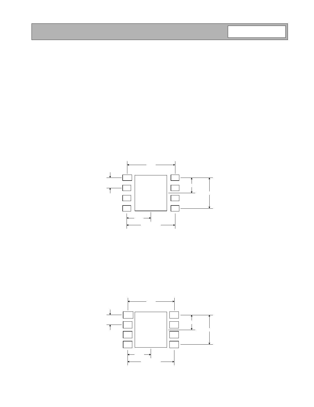
PCB Metal Land Pattern
A = 1.14 x 0.71
B = 1.02 x 0.71 Typ.
C = 3.96 x 4.44
Dimensions in mm.
5.93
Pin 1
A
B
1.27 Typ.
B
B 1.90
C 3.81 Typ.
BB
B
3.00
5.99 Typ.
B
PCB Solder Mask Pattern
Liquid Photo-Imageable (LPI) solder mask is recommended. The solder mask footprint will match what is shown for the
PCB metal land pattern with a 2mil to 3mil expansion to accommodate solder mask registration clearance around all
pads. The center-grounding pad shall also have a solder mask clearance. Expansion of the pads to create solder mask
clearance can be provided in the master data or requested from the PCB fabrication supplier.
A = 1.30 x 0.86
B = 1.17 x 0.86 Typ.
C = 4.11 x 4.60
Dimensions in mm.
Pin 1
1.27 Typ.
A
B
B
5.93
C
B
B 1.90
3.81 Typ.
B
BB
3.00
5.99 Typ.
Rev A4 050912
4-633
11 Page | ||
| Páginas | Total 18 Páginas | |
| PDF Descargar | [ Datasheet RF3807.PDF ] | |
Hoja de datos destacado
| Número de pieza | Descripción | Fabricantes |
| RF3800 | GaAs HBT PRE-DRIVER AMPLIFIER | RF Micro Devices |
| RF3800PCBA-416 | GaAs HBT PRE-DRIVER AMPLIFIER | RF Micro Devices |
| RF3802 | GaAs HBT PRE-DRIVER AMPLIFIER | RF Micro Devices |
| RF3802PCBA-410 | GaAs HBT PRE-DRIVER AMPLIFIER | RF Micro Devices |
| Número de pieza | Descripción | Fabricantes |
| SLA6805M | High Voltage 3 phase Motor Driver IC. |
Sanken |
| SDC1742 | 12- and 14-Bit Hybrid Synchro / Resolver-to-Digital Converters. |
Analog Devices |
|
DataSheet.es es una pagina web que funciona como un repositorio de manuales o hoja de datos de muchos de los productos más populares, |
| DataSheet.es | 2020 | Privacy Policy | Contacto | Buscar |
