|
|
|
PDF ADAU1590 Data sheet ( Hoja de datos )
| Número de pieza | ADAU1590 | |
| Descripción | Class-D Audio Power Amplifier | |
| Fabricantes | Analog Devices | |
| Logotipo | ||
Hay una vista previa y un enlace de descarga de ADAU1590 (archivo pdf) en la parte inferior de esta página. Total 24 Páginas | ||
|
No Preview Available !
Class-D Audio Power Amplifier
ADAU1590
FEATURES
GENERAL DESCRIPTION
Integrated stereo modulator and power stage
0.005% THD + N
101 dB dynamic range
PSRR >55 dB
RDS-ON < 0.3 Ω (per transistor)
Efficiency > 90% (8 Ω)
EMI-optimized modulator
On/off-mute pop-noise suppression
Short-circuit protection
Overtemperature protection
APPLICATIONS
The ADAU1590 is a 2-channel, bridge-tied load (BTL)
switching audio power amplifier with an integrated Σ-Δ
modulator.
The modulator accepts an analog input signal and generates
a switching output to drive speakers directly. A digital,
microcontroller-compatible interface provides control of reset,
mute and PGA gain as well as output signals for thermal and
overcurrent error conditions. The output stage can operate
from supply voltages ranging from 9 V to 15 V. The analog
modulator and digital logic operate from a 3.3 V supply.
Flat panel televisions
PC audio systems
Mini-components
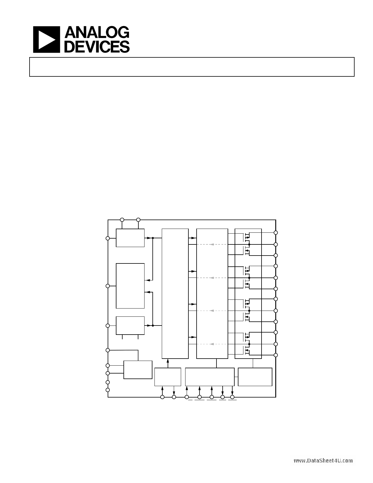
FUNCTIONAL BLOCK DIAGRAM
PGA0 PGA1
www.DataSheet4U.com
AINL
SLC_TH
AINR
AVDD
VREF
AGND
DVDD
DGND
PGA
SLICER
Σ-Δ
MODULATOR
LEVEL SHIFT
AND DEAD
TIME CONTROL
PGA
PGA0 PGA1
VOLTAGE
REFERENCE
fCLK/2
CLOCK
OSCILLATOR
MODE CONTROL
LOGIC
PVDD
A1 OUTL+
A2 PGND
PVDD
B1 OUTL–
B2 PGND
PVDD
C1 OUTR+
C2 PGND
PVDD
D1 OUTR–
D2 PGND
TEMPERATURE
OVERCURRENT
PROTECTION
XTI XTO MO/ST STDN MUTE ERR OTW
Figure 1.
ADAU1590
Rev. 0
Information furnished by Analog Devices is believed to be accurate and reliable. However, no
responsibility is assumed by Analog Devices for its use, nor for any infringements of patents or other
rights of third parties that may result from its use. Specifications subject to change without notice. No
license is granted by implication or otherwise under any patent or patent rights of Analog Devices.
Trademarksandregisteredtrademarksarethepropertyoftheirrespectiveowners.
One Technology Way, P.O. Box 9106, Norwood, MA 02062-9106, U.S.A.
Tel: 781.329.4700
www.analog.com
Fax: 781.461.3113
©2007 Analog Devices, Inc. All rights reserved.
1 page 
ADAU1590
DIGITAL TIMING
Table 5.
Parameter
tWAIT
tINT
tHOLD
tOUTx+/OUTx− SW
tOUTx+/OUTx− MUTE
Min
0.011
101
Typ
10002
650
2503
200
200
Unit
ms
ms
μs
μs
μs
Test Conditions/Comments
Wait time for unmute
Internal mute time
Wait time for shutdown
Time delay after MUTE held high until output starts switching
Time delay after MUTE held low until output stops switching
1 tWAIT MIN and tHOLD MIN are the minimum times for fast turn-on and do not guarantee pop-and-click suppression.
2 tWAIT TYP is the recommended value for minimum pop and click during the unmute of the amplifier. The recommended value is 1 sec. It is calculated using the input
coupling capacitor value and the input resistance of the device. See the Power-Up/Power-Down Sequence section.
3 tHOLD TYP is the recommended value for minimum pop and click during the mute of the amplifier.
STDN
INTERNAL MUTE
MUTE
tINT
tWAIT MIN
OUTx+/OUTx–
NOTES
1. INTERNAL MUTE IS INTERNAL TO CHIP.
Figure 2.Timing Diagram (Minimum)
tHOLD MIN
STDN
INTERNAL MUTE
MUTE
tINT
tWAIT TYP
tHOLD TYP
OUTx+/OUTx–
tOUTx+/OUTx– SW
NOTES
1. INTERNAL MUTE IS INTERNAL TO CHIP.
Figure 3. Timing Diagram (Typical)
tOUTx+/OUTx– MUTE
Rev. 0 | Page 5 of 24
5 Page 
0
–10 0dBr = 9.5W
–20
–30
–40
–50
–60
–70
–80
–90
–100
–110
–120
–130
–140
–150
–160
0 2 4 6 8 10 12 14 16 18 20 22
FREQUENCY (kHz)
Figure 17. FFT @ 1 W, 6 Ω, PVDD = 12 V, PGA = 0 dB, 19 kHz and 20 kHz Sine
0
–10
–20
–30
–40
–50
–60
–70
–80
–90
–100
–110
–120
20
RIGHT TO LEFT
LEFT TO RIGHT
100 1k
FREQUENCY (Hz)
10k
Figure 18. Crosstalk @ 1 W, 6 Ω, PVDD = 12 V, PGA = 0 dB
0
–10
–20
–30
–40
–50
–60
–70
–80
–90
–100
–110
–120
20
RIGHT TO LEFT
LEFT TO RIGHT
100 1k
FREQUENCY (Hz)
10k
Figure 19. Crosstalk @ Full Scale, 6 Ω, PVDD = 12 V, PGA = 0 dB
ADAU1590
0
–10
–20
–30
–40
–50
–60
–70
–80
–90
–100
–110
–120
20
THD + N
THD
100 1k
FREQUENCY (Hz)
10k
Figure 20. THD or THD + N vs. Frequency @ 1 W, 4 Ω, PVDD = 12 V, PGA = 0 dB
0
–10
–20
–30
–40
–50
–60
–70
–80
–90
–100
–110
–120
20
THD + N
THD
100 1k
FREQUENCY (Hz)
10k
Figure 21. THD or THD + N vs. Frequency @ 1 W, 6 Ω, PVDD = 12 V, PGA = 0 dB
0
–10
–20
–30
–40
–50
–60
–70
–80
–90 THD + N
–100
–110
–120
20
THD
100 1k
FREQUENCY (Hz)
10k
Figure 22. THD or THD + N vs. Frequency @ 1 W, 8 Ω, PVDD = 12 V, PGA = 0 dB
Rev. 0 | Page 11 of 24
11 Page | ||
| Páginas | Total 24 Páginas | |
| PDF Descargar | [ Datasheet ADAU1590.PDF ] | |
Hoja de datos destacado
| Número de pieza | Descripción | Fabricantes |
| ADAU1590 | Class-D Audio Power Amplifier | Analog Devices |
| ADAU1592 | Class-D Audio Power Amplifier | Analog Devices |
| Número de pieza | Descripción | Fabricantes |
| SLA6805M | High Voltage 3 phase Motor Driver IC. |
Sanken |
| SDC1742 | 12- and 14-Bit Hybrid Synchro / Resolver-to-Digital Converters. |
Analog Devices |
|
DataSheet.es es una pagina web que funciona como un repositorio de manuales o hoja de datos de muchos de los productos más populares, |
| DataSheet.es | 2020 | Privacy Policy | Contacto | Buscar |