|
|
|
PDF 34717 Data sheet ( Hoja de datos )
| Número de pieza | 34717 | |
| Descripción | Dual Switch-Mode Power Supply | |
| Fabricantes | Freescale Semiconductor | |
| Logotipo | ||
Hay una vista previa y un enlace de descarga de 34717 (archivo pdf) en la parte inferior de esta página. Total 30 Páginas | ||
|
No Preview Available !
Freescale Semiconductor
Advance Information
5.0 A 1.0 MHz Fully Integrated
Dual Switch-Mode Power
Supply
Document Number: MC34717
Rev 5.0, 12/2014
34717
The 34717 is a highly integrated, space-efficient, low cost, dual
synchronous buck switching regulator with integrated N-channel
power MOSFETs. It is a high performance dual point-of-load (PoL)
power supply with many desired features for the 3.3 and 5.0 V
environments.
Both channels can provide up to 5.0 A of continuous output current
capability with high efficiency and tight output regulation. The second
channel has the ability to track an external reference voltage in
different configurations.
The 34717 SMARTMOS device offers the designer the flexibility of
many control, supervisory, and protection functions to allow for easy
implementation of complex designs. It is housed in a Pb-free,
thermally enhanced, and space efficient 26 pin exposed pad QFN.
Features
• 50 m integrated N-channel power MOSFETs
• Input voltage operating range from 3.0 to 6.0 V
• 1% accurate output voltages, ranging from 0.7 to 3.6 V
• The second output has voltage tracking capability in different
configurations
• Programmable switching frequency range from 200 kHz to
1.0 MHz
• Programmable soft start timing
• Over-current limit and short-circuit protection
• Thermal shutdown
• Output overvoltage and undervoltage detection
• Active low power good output signal
• Active low shutdown input.
DUAL SWITCH-MODE POWER SUPPLY
EP SUFFIX (PB_FREE)
98ASA00702D
26-PIN QFN
ORDERING INFORMATION
Device
Temperature
Range (TA)
Package
MC34717EP/R2 -40 °C to 85 °C
26 QFN
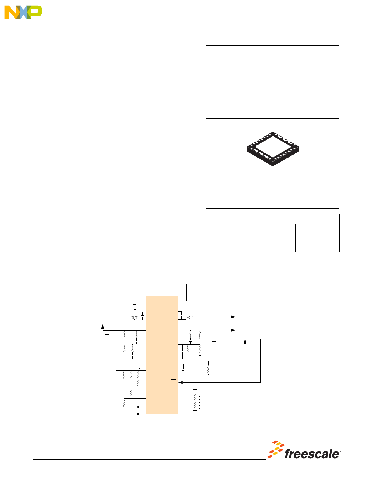
3.0 TO 6.0 V VIN
VOUT1
34717
VIN PVIN2
PVIN1
BOOT1 BOOT2
SW1 SW2
VOUT1 VOUT2
VOUT1
VOUT2
MCU
INV1 INV2
COMP1
PGND1
VDDI
FREQ
ILIM1
COMP2
PGND2
PG
SD
ILIM2 VREFIN
GND
VIN
VMASTER
Optional
Figure 1. 34717 Simplified Application Diagram
* This document contains certain information on a new product.
Specifications and information herein are subject to change without notice.
© Freescale Semiconductor, Inc., 2007-2014. All rights reserved.
1 page 
ELECTRICAL CHARACTERISTICS
MAXIMUM RATINGS
ELECTRICAL CHARACTERISTICS
MAXIMUM RATINGS
Table 2. Maximum Ratings
All voltages are with respect to ground unless otherwise noted. Exceeding these ratings may cause a malfunction or
permanent damage to the device.
Ratings
Symbol
Value
Unit
ELECTRICAL RATINGS
Input Supply Voltage (VIN) Pin
High-side MOSFET Drain Voltage (PVIN1, PVIN2) Pins
Switching Node (SW1, SW2) Pins
BOOT1, BOOT2 Pins (Referenced to SW1, SW2 Pins Respectively)
PG, VOUT1, VOUT2, and SD Pins
VIN
PVIN
VSW
VBOOT - VSW
-
-0.3 to 7.0
-0.3 to 7.0
-0.3 to 7.0
-0.3 to 7.0
-0.3 to 7.0
V
V
V
V
V
VDDI, FREQ, ILIM1, ILIM2, INV1, INV2, COMP1, COMP2, and VREFIN Pins
-
-0.3 to 3.0
V
Channel 1 Continuous Output Current(1)
Channel 2 Continuous Output Current(1)
ESD Voltage(2)
Human Body Model
Machine Model (MM)
Charge Device Model
IOUT1
IOUT2
VESD1
VESD2
VESD3
+5.0
+5.0
±2000
±200
±750
A
A
V
THERMAL RATINGS
Operating Ambient Temperature(3)
TA
-40 to 85
°C
Storage Temperature
Peak Package Reflow Temperature During Reflow(4),(5)
TSTG
TPPRT
-65 to +150
Note 5
°C
°C
Maximum Junction Temperature
Power Dissipation (TA = 85°C)(6)
TJ(MAX)
PD
+150
2.03
°C
W
Notes
1. Continuous output current capability so long as TJ is TJ(MAX).
2. ESD testing is performed in accordance with the Human Body Model (HBM) (CZAP = 100 pF, RZAP = 1500 ), the Machine Model (MM)
(CZAP = 200 pF, RZAP = 0 ), and the Charge Device Model (CDM), Robotic (CZAP = 4.0 pF).
3. The limiting factor is junction temperature, taking into account power dissipation, thermal resistance, and heatsinking.
4. Pin soldering temperature limit is for 10 seconds maximum duration. Not designed for immersion soldering. Exceeding these limits may
cause malfunction or permanent damage to the device.
5. Freescale’s Package Reflow capability meets Pb-free requirements for JEDEC standard J-STD-020C. For Peak Package Reflow
Temperature and Moisture Sensitivity Levels (MSL), Go to www.freescale.com, search by part number [e.g. remove prefixes/suffixes
and enter the core ID to view all orderable parts. (i.e. MC33xxxD enter 33xxx), and review parametrics.
6. Maximum power dissipation at indicated ambient temperature.
Analog Integrated Circuit Device Data
Freescale Semiconductor
34717
5
5 Page 
ELECTRICAL CHARACTERISTICS
DYNAMIC ELECTRICAL CHARACTERISTICS
Table 4. Dynamic Electrical Characteristics
Characteristics noted under conditions 3.0 V VIN 6.0 V, -40 C TA 85 C, GND = 0 V, unless otherwise noted. Typical
values noted reflect the approximate parameter means at TA = 25 °C under nominal conditions, unless otherwise noted.
Characteristic
Symbol
Min
Typ
Max Unit
OSCILLATOR (FREQ)(20)
Oscillator Default Switching Frequency
(FREQ = GND)
FSW - 1.0 - MHz
Oscillator Switching Frequency Range
CONTROL AND SUPERVISORY (SD, PG)
FSW
200
-
1000
kHz
PG Reset Delay
Thermal Shutdown Retry Timeout Period(21)
tPGRESET
8.0
-
12 ms
tTIMEOUT
80
- 120 ms
Notes
20. Oscillator frequency is ±10%
21. Design information only, this parameter is not production tested.
Analog Integrated Circuit Device Data
Freescale Semiconductor
34717
11
11 Page | ||
| Páginas | Total 30 Páginas | |
| PDF Descargar | [ Datasheet 34717.PDF ] | |
Hoja de datos destacado
| Número de pieza | Descripción | Fabricantes |
| 34710 | Adjustable Dual Output Switching Power Supply | Motorola Inc |
| 34712 | DDR Switch-Mode Power Supply | Freescale Semiconductor |
| 34713 | Single Switch-Mode Power Supply | Freescale Semiconductor |
| 34716 | Dual Switch-Mode DDR Power Supply | Freescale Semiconductor |
| Número de pieza | Descripción | Fabricantes |
| SLA6805M | High Voltage 3 phase Motor Driver IC. |
Sanken |
| SDC1742 | 12- and 14-Bit Hybrid Synchro / Resolver-to-Digital Converters. |
Analog Devices |
|
DataSheet.es es una pagina web que funciona como un repositorio de manuales o hoja de datos de muchos de los productos más populares, |
| DataSheet.es | 2020 | Privacy Policy | Contacto | Buscar |