|
|
|
PDF AD8147 Data sheet ( Hoja de datos )
| Número de pieza | AD8147 | |
| Descripción | (AD8146 - AD8148) Triple Differential Driver | |
| Fabricantes | Analog Devices | |
| Logotipo | ||
Hay una vista previa y un enlace de descarga de AD8147 (archivo pdf) en la parte inferior de esta página. Total 24 Páginas | ||
|
No Preview Available !
Data Sheet
FEATURES
Triple high speed fully differential driver
700 MHz, −3 dB, 2 V p-p bandwidth (AD8146/AD8148)
600 MHz, −3 dB, 2 V p-p bandwidth (AD8147)
200 MHz, 0.1 dB, 2 V p-p bandwidth
3000 V/μs slew rate
Fixed gain (AD8146/AD8147: G = 2, AD8148: G = 4)
Differential or single-ended input to differential output
Can be used as differential-to-differential receiver
Drives one or two 100 Ω UTP cables
Adjustable output common-mode voltage (AD8146)
Internal common-mode feedback network
Output balance error −50 dB @ 50 MHz
On-chip, sync-on common-mode encoding (AD8147/AD8148)
Output pull-down feature for line isolation
Low power: 57 mA @ 5 V for 3 drivers (AD8146)
Wide supply voltage range: +5 V to ±5 V
Available in a small 4 mm × 4 mm LFCSP
APPLICATIONS
QXGA or 1080p video transmission
KVM networking
Video over unshielded twisted pair (UTP)
Differential signal multiplexing
Triple Differential Driver
for Wideband Video
AD8146/AD8147/AD8148
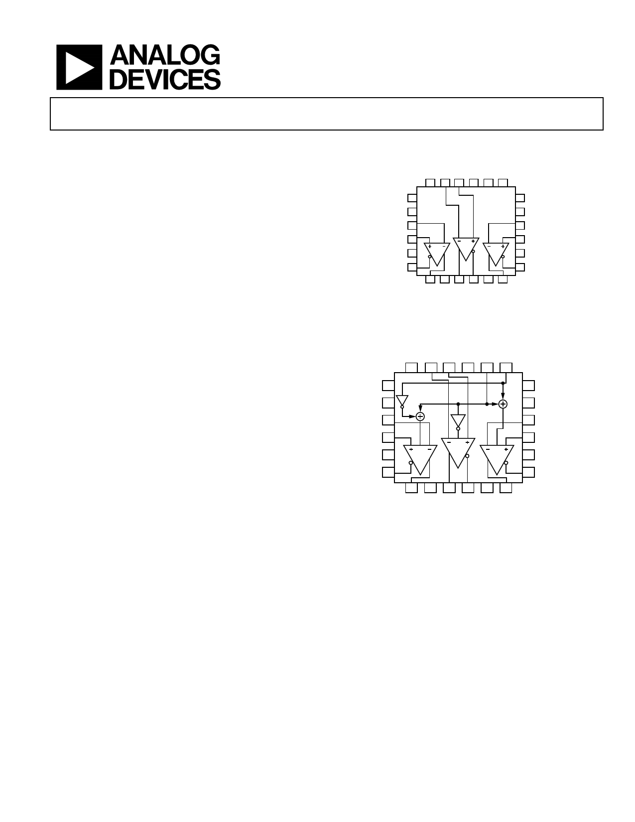
FUNCTIONAL BLOCK DIAGRAMS
OPD 1
VS– 2
–IN A 3
+IN A 4
VS– 5
–OUT A 6
24 23 22 21 20 19
A
78
AD8146 18 VOCMC
17 VS+
16 –IN C
15 +IN C
B
C 14 VS–
13 –OUT C
9 10 11 12
Figure 1.
OPD 1
VS– 2
–IN R 3
+IN R 4
VS– 5
–OUT R 6
24 23 22 21 20 19
AD8147/
AD8148
×2
B
AC
7 8 9 10 11 12
18 SYNC LEVEL
17 VS+ (SYNC)
16 –IN B
15 +IN B
14 VS–
13 –OUT B
GENERAL DESCRIPTION
The AD8146/AD8147/AD8148 are high speed triple, differential or
single-ended input to differential output drivers. The AD8146
and AD8147 have a fixed gain of 2, and the AD8148 has a fixed
gain of 4. They are all specifically designed for the highest
resolution component video signals but can be used for any
type of analog signals or high speed data transmission over
either Category 5 UTP cable or differential printed circuit
board (PCB) transmission lines.
These drivers can be used with the AD8145 triple differential-
to-singled-ended receiver, and the AD8117 crosspoint switch to
produce a video distribution system capable of supporting
UXGA or 1080p signals.
Manufactured on the Analog Devices, Inc. second generation
XFCB bipolar process, the drivers have large signal bandwidths
Rev. B
Document Feedback
Information furnished by Analog Devices is believed to be accurate and reliable. However, no
responsibility is assumed by Analog Devices for its use, nor for any infringements of patents or other
rights of third parties that may result from its use. Specifications subject to change without notice. No
license is granted by implication or otherwise under any patent or patent rights of Analog Devices.
Trademarksandregisteredtrademarksarethepropertyoftheirrespectiveowners.
Figure 2.
of 700 MHz and fast slew rates. They have an internal common-
mode feedback feature that provides output amplitude and
phase matching that is balanced to −60 dB at 50 MHz, suppressing
even-order harmonics and minimizing radiated
electromagnetic interference (EMI).
The common-mode voltage of each AD8146 output can be set
to any level, allowing transmission of signals over the common-
mode voltages. The AD8147 and AD8148 encode the vertical
and horizontal sync signals on the common-mode voltages of
the outputs. All outputs can be independently set to low voltage
states to be used with series diodes for line isolation, allowing
easy differential multiplexing over the same twisted pair cable.
The AD8146/AD8147/AD8148 are available in a 24-lead LFCSP
and operate over a temperature range of −40°C to +85°C.
One Technology Way, P.O. Box 9106, Norwood, MA 02062-9106, U.S.A.
Tel: 781.329.4700 ©2007–2014 Analog Devices, Inc. All rights reserved.
Technical Support
www.analog.com
1 page 
Data Sheet
AD8146/AD8147/AD8148
VS = +5 V or ±2.5 V; VOCM = midsupply (AD8146); SYNC LEVEL = 0 V (AD8147/AD8148); T = 25°C; RL,dm = 200 Ω, unless otherwise noted.
TMIN to TMAX = −40°C to +85°C.
Table 2.
Parameter
DIFFERENTIAL INPUT AC
Dynamic Performance
−3 dB Small Signal Bandwidth
−3 dB Large Signal Bandwidth
Bandwidth for 0.1 dB Flatness
DIFFERENTIAL INPUT DC
Input Common-Mode Voltage Range
Input Resistance
Input Capacitance
DC CMRR
DIFFERENTIAL OUTPUT
Differential Signal Gain
Output Voltage Swing
Output Offset Voltage
Output Offset Drift
Output Balance Error
Output Voltage Noise (RTO)
Output Short-Circuit Current
VOCM DYNAMIC PERFORMANCE (AD8146
ONLY)
−3 dB Bandwidth
Slew Rate
DC Gain
Conditions
Min
VO = 0.2 V p-p,
AD8146
AD8147/AD8148
VO = 2 V p-p,
AD8147
AD8146/AD8148
VO = 2 V p-p,
AD8146/AD8147
AD8148
Differential
Single-ended input
AD8146/AD8147
AD8148
Differential
ΔVOUT, dm/ΔVIN, cm; ΔVIN, cm = ±1 V,
AD8146/AD8147/AD8148
ΔVOUT, dm/ΔVIN, dm; ΔVIN, dm = ±1 V,
AD8146/AD8147
ΔVOUT, dm/ΔVIN, dm; ΔVIN, dm = ±1 V
AD8148
Each single-ended output, VS = ±2.5 V
TMIN to TMAX
ΔVOUT, cm/ΔVIN, dm, ΔVOUT, dm = 2 V p-p,
f = 50 MHz
AD8146/AD8147
AD8148
DC
AD8146/AD8148
AD8147
f = 1 MHz
AD8146/AD8147
AD8148
Short to GND, source/sink
1.94
3.80
−1.17
−17
ΔVOCM = 100 mV p-p
VOCM = −1 V to +1 V, 25% to 75%
ΔVOCM = ±1 V
0.98
Typ Max Unit
870
680
590
620
165
200
0 to 5
1.0
750
833
2
MHz
MHz
MHz
MHz
MHz
MHz
V
kΩ
Ω
Ω
pF
−49/−45/−49 dB
2.00
4.00
+1.24
+17
±8
−53
−49
V/V
V/V
V
mV
µV/°C
dB
dB
−41
−44
25
42
+63/−48
310
800
1.00
dB
dB
nV/√Hz
nV/√Hz
mA
MHz
V/µs
V/V
Rev. B | Page 5 of 24
5 Page 
Data Sheet
1.5
VS = ±2.5V
1.0
0.5 VS = ±5.0V
VOUT, dm = 2V p-p
0
–0.5
–1.0
–1.5
0 2 4 6 8 10 12 14 16 18 20
TIME (ns)
Figure 12. AD8146/AD8147 Large Signal Transient Response for Various Supplies
150
VS = ±2.5V
100
50 VS = ±5.0V
VOUT, dm = 0.2V p-p
0
–50
–100
–150
0 2 4 6 8 10 12 14 16 18 20
TIME (ns)
Figure 13. AD8146/AD8147 Small Signal Transient Response for Various Supplies
–20
ΔVOUT, cm/ΔVOUT, dm
–25 ΔVOUT, dm = 2V p-p
–30
AD8146
–35
–40
–45
–50 AD8147
–55
AD8148
–60
–65
–70
1
10 100
FREQUENCY (MHz)
Figure 14. Output Balance vs. Frequency
1000
AD8146/AD8147/AD8148
1.5
VS = ±2.5V
1.0
0.5 VS = ±5.0V
VOUT, dm = 2V p-p
0
–0.5
–1.0
–1.5
0 2 4 6 8 10 12 14 16 18 20
TIME (ns)
Figure 15. AD8148 Large Signal Transient Response for Various Supplies
150
VS = ±2.5V
100
50 VS = ±5.0V
VOUT, dm = 0.2V p-p
0
–50
–100
–150
0 2 4 6 8 10 12 14 16 18 20
TIME (ns)
Figure 16. AD8148 Small Signal Transient Response for Various Supplies
–20
ΔVOUT, dm/ΔVIN, cm
ΔVIN, cm = 2V p-p
–30
–40
–50
AD8148
AD8147
–60
AD8146
–70
–80
1
10 100
FREQUENCY (MHz)
Figure 17. CMRR vs. Frequency
1000
Rev. B | Page 11 of 24
11 Page | ||
| Páginas | Total 24 Páginas | |
| PDF Descargar | [ Datasheet AD8147.PDF ] | |
Hoja de datos destacado
| Número de pieza | Descripción | Fabricantes |
| AD8141 | Triple Differential Drivers | Analog Devices |
| AD8142 | Triple Differential Drivers | Analog Devices |
| AD8143 | Triple Differential Receiver | Analog Devices |
| AD8145 | Triple Differential Receiver | Analog Devices |
| Número de pieza | Descripción | Fabricantes |
| SLA6805M | High Voltage 3 phase Motor Driver IC. |
Sanken |
| SDC1742 | 12- and 14-Bit Hybrid Synchro / Resolver-to-Digital Converters. |
Analog Devices |
|
DataSheet.es es una pagina web que funciona como un repositorio de manuales o hoja de datos de muchos de los productos más populares, |
| DataSheet.es | 2020 | Privacy Policy | Contacto | Buscar |