|
|
|
PDF AD1974 Data sheet ( Hoja de datos )
| Número de pieza | AD1974 | |
| Descripción | ADC | |
| Fabricantes | Analog Devices | |
| Logotipo | ||
Hay una vista previa y un enlace de descarga de AD1974 (archivo pdf) en la parte inferior de esta página. Total 24 Páginas | ||
|
No Preview Available !
4 ADC with PLL,
192 kHz, 24-Bit Codec
AD1974
FEATURES
Phase-locked loop generated or direct master clock
Low EMI design
107 dB dynamic range and SNR
−94 dB THD + N
Single 3.3 V supply
Tolerance for 5 V logic inputs
Supports 24 bits and 8 kHz to 192 kHz sample rates
Differential ADC input
Log volume control with autoramp function
SPI®-controllable for flexibility
Software-controllable clickless mute
Software power-down
Right justified, left justified, I2S, and TDM modes
Master and slave modes up to 16-channel input/output
Available in a 48-lead LQFP
APPLICATIONS
Automotive audio systems
Home Theater Systems
Set-top boxes
www.DataSheet4U.com Digital audio effects processors
GENERAL DESCRIPTION
The AD1974 is a high performance, single-chip codec that pro-
vides four analog-to-digital converters (ADCs) with differential
inputs using the Analog Devices, Inc. patented multibit sigma-
delta (Σ-Δ) architecture. An SPI port is included, allowing a
microcontroller to adjust volume and many other parameters.
The AD1974 operates from 3.3 V digital and analog supplies.
The AD1974 is available in a single-ended output 48-lead LQFP.
The AD1974 is designed for low EMI. This consideration is
apparent in both the system and circuit design architectures.
By using the on-board phase-locked loop (PLL) to derive the
master clock from the LR clock or from an external crystal,
the AD1974 eliminates the need for a separate high frequency
master clock and can also be used with a suppressed bit clock.
The ADCs are designed using the latest continuous time archi-
tectures from Analog Devices to further minimize EMI. By
using 3.3 V supplies, power consumption is minimized, further
reducing emissions.
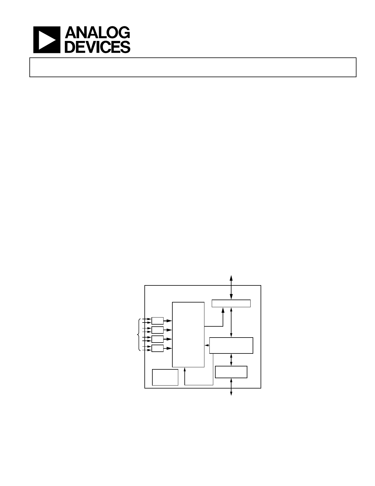
FUNCTIONAL BLOCK DIAGRAM
DIGITAL AUDIO
INPUT/OUTPUT
ANALOG
AUDIO
INPUTS
AD1974
SERIAL DATA PORT
ADC
ADC
ADC
ADC
QUAD
DEC
FILTER
48kHz/
96kHz/192kHz
SDATA
OUT
CLOCKS
TIMING MANAGEMENT
AND CONTROL
(CLOCK AND PLL)
PRECISION
VOLTAGE
REFERENCE
CONTROL PORT
SPI
12.48MHz
Figure 1.
CONTROL DATA
INPUT/OUTPUT
Rev. 0
Information furnished by Analog Devices is believed to be accurate and reliable. However, no
responsibility is assumed by Analog Devices for its use, nor for any infringements of patents or other
rights of third parties that may result from its use. Specifications subject to change without notice. No
license is granted by implication or otherwise under any patent or patent rights of Analog Devices.
Trademarksandregisteredtrademarksarethepropertyoftheirrespectiveowners.
One Technology Way, P.O. Box 9106, Norwood, MA 02062-9106, U.S.A.
Tel: 781.329.4700
www.analog.com
Fax: 781.461.3113
©2007 Analog Devices, Inc. All rights reserved.
1 page 
POWER SUPPLY SPECIFICATIONS
Table 5.
Parameter
SUPPLIES
Voltage
Digital Current
Normal Operation
Power-Down
Analog Current
Normal Operation
Power-Down
DISSIPATION
Operation
All Supplies
Digital Supply
Analog Supply
Power-Down, All Supplies
POWER SUPPLY REJECTION RATIO
Signal at Analog Supply Pins
Conditions/Comments
DVDD
AVDD
MCLK = 256 fS
fS = 48 kHz
fS = 96 kHz
fS = 192 kHz
fS = 48 kHz to 192 kHz
MCLK = 256 fS, 48 kHz
1 kHz, 200 mV p-p
20 kHz, 200 mV p-p
AD1974
Min Typ Max Unit
3.0 3.3 3.6
3.0 3.3 3.6
56
65
95
2.0
74
23
V
V
mA
mA
mA
mA
mA
mA
429 mW
185 mW
244 mW
83 mW
50 dB
50 dB
DIGITAL FILTERS
Table 6.
Parameter
ADC DECIMATION FILTER
Pass Band
Pass-Band Ripple
Transition Band
Stop Band
Stop-Band Attenuation
Group Delay
Mode
All modes @ 48 kHz
Factor
0.4375 fS
0.5 fS
0.5625 fS
22.9844 fS
Min Typ
21
±0.015
24
27
79
479
Max
Unit
kHz
dB
kHz
kHz
dB
μs
TIMING SPECIFICATIONS
−40°C < TA < +130°C, DVDD = 3.3 V ± 10%.
Table 7.
Parameter
INPUT MASTER CLOCK (MCLK)
AND RESET
tMH
tMH
Condition
MCLK duty cycle
fMCLK
fMCLK
tPDR
tPDRR
MCLK frequency
Low
Recovery
Comments
Min Max Unit
ADC clock source = PLL clock @ 256 fS, 384 fS, 512 fS, 768 fS 40 60 %
ADC clock source = direct MCLK @ 512 fS (bypass
on-chip PLL)
40 60 %
PLL mode, 256 fS reference
6.9 13.8 MHz
Direct 512 fS mode
27.6 MHz
15 ns
Reset to active output
4096
tMCLK
Rev. 0 | Page 5 of 24
5 Page 
THEORY OF OPERATION
ANALOG-TO-DIGITAL CONVERTERS (ADCS)
There are four ADC channels in the AD1974 configured as two
stereo pairs with differential inputs. The ADCs can operate at a
nominal sample rate of 48 kHz, 96 kHz, or 192 kHz. The ADCs
include on-board digital antialiasing filters with a 79 dB stop-
band attenuation and a linear phase response, operating at
an oversampling ratio of 128 (48 kHz, 96 kHz, and 192 kHz
modes). Digital outputs are supplied through two serial data
output pins (one for each stereo pair) as well as a common
frame (ALRCLK) and bit clock (ABCLK). Alternatively, one
of the time division multiplexed (TDM) modes can be used
to access up to 16 channels on a single TDM data line.
The ADCs must be driven from a differential signal source for
best performance. The input pins of the ADCs connect to inter-
nal switched capacitors. To isolate the external driving op amp
from the glitches caused by the internal switched capacitors,
each input pin should be isolated by using a series connected,
external, 100 Ω resistor together with a 1 nF capacitor connected
from each input to ground. This capacitor must be of high quality,
for instance, a ceramic NPO capacitor or a polypropylene film
capacitor.
The differential inputs have a nominal common-mode voltage
of 1.5 V. The voltage at the common-mode reference pin (CM)
can be used to bias external op amps to buffer the input signals
(see the Power Supply and Voltage Reference section). The inputs
can also be ac-coupled and do not need an external dc bias to CM.
A digital high-pass filter can be switched in line with the ADCs
under serial control to remove residual dc offsets. It has a 1.4 Hz,
6 dB per octave cutoff at a 48 kHz sample rate. The cutoff fre-
quency scales directly with sample frequency.
The voltage at CM can be used to bias the external op amps that
buffer the output signals (see the Power Supply and Voltage
Reference section).
CLOCK SIGNALS
The on-chip PLL can be selected to reference the input sample
rate from either the LRCLK or AUXLRCK pins or 256, 384, 512,
or 768 times the sample rate, referenced to the 48 kHz mode from
the MCLKI/XI pin. The default at power-up is 256 × fS from
MCLKI. In 96 kHz mode, the master clock frequency stays
at the same absolute frequency; therefore, the actual mul-
tiplication rate is divided by 2. In 192 kHz mode, the actual
multiplication rate is divided by 4. For example, if the AD1974
is programmed in 256 × fS mode, the frequency of the master
clock input is 256 × 48 kHz = 12.288 MHz. If the AD1974 is
then switched to 96 kHz operation (by writing to the SPI or
I2C port), the frequency of the master clock should remain at
12.288 MHz (128 × fS). In 192 kHz mode, this becomes 64 × fS.
AD1974
The internal clock for the ADCs is 256 × fS for all clock modes.
By default, the on-board PLL generates this internal master clock
from an external clock. A direct 512 × fS (referenced to 48 kHz
mode) master clock can be used for the ADCs if selected in the
PLL and Clock Control 1 register.
Note that it is not possible to use a direct clock for the ADCs
set to the 192 kHz mode. It is required that the on-chip PLL be
used in this mode.
The PLL can be powered down in the PLL and Clock Control 0
register. To ensure reliable locking when changing PLL modes,
or if the reference clock is unstable at power-on, power down
the PLL and then power it back up when the reference clock has
stabilized.
The internal MCLK can be disabled in the PLL and Clock Control
0 register to reduce power dissipation when the AD1974 is idle.
The clock should be stable before it is enabled. Unless a stand-
alone mode is selected (see the Serial Control Port section), the
clock is disabled by reset and must be enabled by writing to the
SPI or I2C port for normal operation.
To maintain the highest performance possible, it is recom-
mended that the clock jitter of the internal master clock signal
be limited to less than 300 ps rms time interval error (TIE). Even
at these levels, extra noise or tones can appear in the outputs if
the jitter spectrum contains large spectral peaks. If the internal
PLL is not being used, it is highly recommended that an inde-
pendent crystal oscillator generate the master clock. In addition,
it is especially important that the clock signal should not be
passed through an FPGA, CPLD, DSP, or other large digital
chip before being applied to the AD1974. In most cases, this
induces clock jitter due to the sharing of common power and
ground connections with other unrelated digital output signals.
When the PLL is used, jitter in the reference clock is attenuated
above a certain frequency depending on the loop filter.
RESET AND POWER-DOWN
The reset pin sets all the control registers to their default settings.
To avoid pops, reset does not power down the analog outputs.
After reset is deasserted, and the PLL acquires a lock condition,
an initialization routine runs inside the AD1974. This initializa-
tion lasts for approximately 256 master clock cycles.
The PLL and Clock Control 0 register and the ADC Control 1
register power down their respective sections using power down
bits. All other register settings are retained. The PD/RST pin
should be pulled low by an external resistor to guarantee proper
startup.
Rev. 0 | Page 11 of 24
11 Page | ||
| Páginas | Total 24 Páginas | |
| PDF Descargar | [ Datasheet AD1974.PDF ] | |
Hoja de datos destacado
| Número de pieza | Descripción | Fabricantes |
| AD1970 | Digital BTSC Encoder | Analog Devices |
| AD1974 | ADC | Analog Devices |
| Número de pieza | Descripción | Fabricantes |
| SLA6805M | High Voltage 3 phase Motor Driver IC. |
Sanken |
| SDC1742 | 12- and 14-Bit Hybrid Synchro / Resolver-to-Digital Converters. |
Analog Devices |
|
DataSheet.es es una pagina web que funciona como un repositorio de manuales o hoja de datos de muchos de los productos más populares, |
| DataSheet.es | 2020 | Privacy Policy | Contacto | Buscar |