|
|
|
PDF XC25BS6 Data sheet ( Hoja de datos )
| Número de pieza | XC25BS6 | |
| Descripción | Divider Signal Output Clock Generator ICs | |
| Fabricantes | Torex Semiconductor | |
| Logotipo | ||
Hay una vista previa y un enlace de descarga de XC25BS6 (archivo pdf) en la parte inferior de esta página. Total 4 Páginas | ||
|
No Preview Available !
XC25BS6 Series
Divider Signal Output Clock Generator ICs with Built-In Crystal Oscillator Circuit
Preliminary
September 17, 2003 V1
CMOS
Low Operating Supply Voltage
Output Frequency
Oscillation Frequency
Built-In Divider Circuit
Output
Ultra Small Package
Chip Form
Low Power Consumption
2.3V (MIN.)
32.768kHz
2MHz ~ 36MHz (fundamental)
Selectable from divisions of
1024, 512, 256, 128
3-State
SOT-26
APPLICATIONS
z Crystal Oscillation Modules
z Clocks for Micro-computers, DSPs, etc.
z Communication Equipment
z Various System Clocks
z Clock Time-Base
GENERAL DESCRIPTION
The XC25BS6 is a low operating voltage, low current consumption
series of CMOS ICs with built-in crystal oscillator and divider circuits
designed for clock generators. Oscillation capacitors Cg and Cd are
externally set up.
Output is selectable from any one of the following values for f0:f0/1024,
f0/512, f0/256, and f0/128.
With oscillation feedback resistors built-in, it is possible to configure a
stable fundamental oscillator using about 10pF of external oscillation
capacitor and an external crystal.
The series has a stand-by function. The oscillation completely stops in
the stand-by state and output will be one of high-impedance.
FEATURES
Oscillation Frequency
Divider Ratio
Output
Operating Supply
Voltage Range
Supply Current
Chip Form
Package
2MHz ~ 36MHz (fundamental)
- Oscillation feedback resistor built-in
- External oscillation capacitor
f0/1024, f0/ 512, f0/256, f0/128
3-State
2.3 ~ 4.0V
0.5µA (MAX.) when stand-by mode
Chip size 1.3 x 0.8mm
SOT-26 mini mold
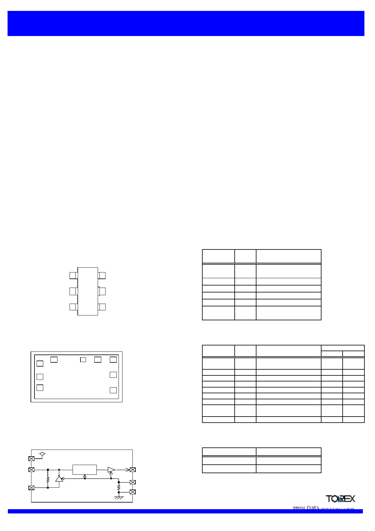
PIN CONFIGURATION
/XT 1
VSS 2
Q0 3
6 XT
5 VDD
4 CE
PIN ASSIGNMENT
PIN
PIN NUMBER NAME
FUNCTIONS
1
/ XT
Crystal Oscillator
Connection (Output)
2 VSS
Ground
3 Q0
Clock Output
4 CE Stand-by Control *
5 VDD
Power Supply
6
XT
Crystal Oscillator
Connection (Input)
* The stand-by control pin (pin #4) has a pull-down resistor built-in.
PAD LAYOUT FOR CHIP FORM
(1300,800)
VSS
/XT
(NC) VSS Q0
VDD
VDD
XT CE
(0,0) Chip Size
: 1300 x 800µm
Chip Thickness : 280±20µm
Chip Back : VDD level
Pad Aperture : 88 x 88 µm
Note)
There are two VSS
pads and two VDD
pads. Please connect
both VSS pads to
GND, and connect
both VDD pads to a
power supply.
PAD LOCATIONS
PIN
PIN NUMBER
NAME
1 / XT
2 VSS
3 (NC)
4 VSS
5 Q0
6 VDD
7 CE
8 XT
9 VDD
FUNCTIONS
Crystal Oscillator
Connection (Output)
Ground
No Connection
Ground
Clock Output
Power Supply
Stand-by Control *
Crystal Oscillator
Connection (Input)
Power Supply
(Unit:µm)
PAD DIMENSIONS
XY
128.0
328.0
741.0
952.0
1172.0
1172.0
1172.0
610.0
672.0
672.0
672.0
672.0
430.0
189.0
128.0
128.0
187.0
399.0
* The stand-by control pin (pin #4) has a pull-down resistor built-in.
BLOCK DIAGRAM
VDD
/XT
Counter
XT
Q0
CE
VSS
CE, Q0 PIN FUNCTION
CE
'H'
'L' or Open
Q0
Clock Output
High Impedance
Semiconductor Ltd.
Data Sheet
1
1 page | ||
| Páginas | Total 4 Páginas | |
| PDF Descargar | [ Datasheet XC25BS6.PDF ] | |
Hoja de datos destacado
| Número de pieza | Descripción | Fabricantes |
| XC25BS3 | CMOS Low Power Consumption | Torex Semiconductor |
| XC25BS5 | PLL Clock Generator ICs with Built-In Divider/Multiplier Circuits (For Low Frequency range) | Torex Semiconductor |
| XC25BS5001ML | PLL Clock Generator ICs with Built-In Divider/Multiplier Circuits (For Low Frequency range) | Torex Semiconductor |
| XC25BS5001MR | PLL Clock Generator ICs with Built-In Divider/Multiplier Circuits (For Low Frequency range) | Torex Semiconductor |
| Número de pieza | Descripción | Fabricantes |
| SLA6805M | High Voltage 3 phase Motor Driver IC. |
Sanken |
| SDC1742 | 12- and 14-Bit Hybrid Synchro / Resolver-to-Digital Converters. |
Analog Devices |
|
DataSheet.es es una pagina web que funciona como un repositorio de manuales o hoja de datos de muchos de los productos más populares, |
| DataSheet.es | 2020 | Privacy Policy | Contacto | Buscar |