|
|
|
PDF AD9865 Data sheet ( Hoja de datos )
| Número de pieza | AD9865 | |
| Descripción | Broadband Modem Mixed-Signal Front End | |
| Fabricantes | Analog Devices | |
| Logotipo | ||
Hay una vista previa y un enlace de descarga de AD9865 (archivo pdf) en la parte inferior de esta página. Total 30 Páginas | ||
|
No Preview Available !
Data Sheet
Broadband Modem Mixed-Signal Front End
AD9865
FEATURES
Low cost 3.3 V CMOS MxFETM for broadband modems
10-bit D/A converter
2×/4× interpolation filter
200 MSPS DAC update rate
Integrated 23 dBm line driver with 19.5 dB gain control
10-bit, 80 MSPS A/D converter
−12 dB to +48 dB low noise RxPGA (< 3.0 nV/rtHz)
Third order, programmable low-pass filter
Flexible digital data path interface
Half- and full-duplex operation
Backward-compatible with AD9975 and AD9875
Various power-down/reduction modes
Internal clock multiplier (PLL)
2 auxiliary programmable clock outputs
Available in 64-lead chip scale package or bare die
APPLICATIONS
Powerline networking
VDSL and HPNA
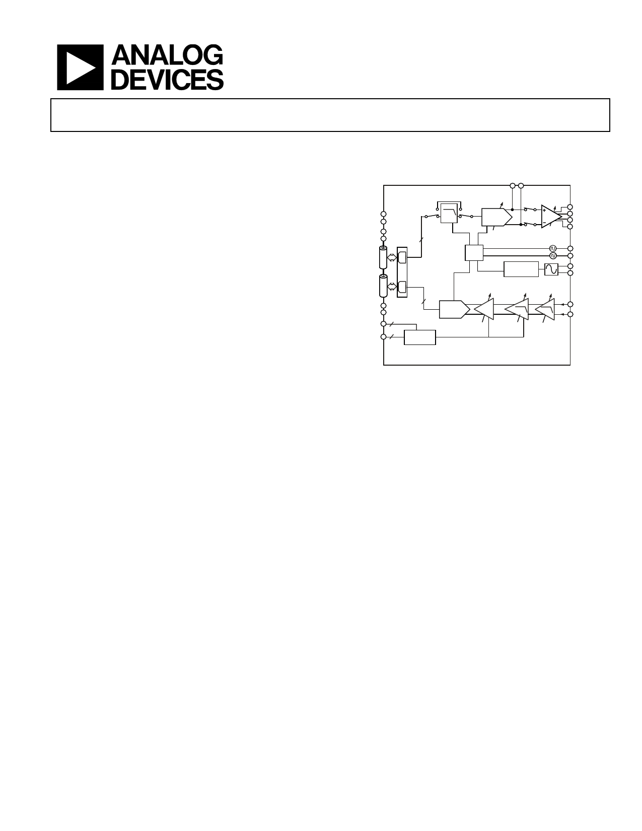
FUNCTIONAL BLOCK DIAGRAM
PWR DWN
MODE
TXEN/SYNC
TXCLK
ADIO[9:4]/
Tx[5:0]
ADIO[3:0]/
Rx[5:0]
RXE/SYNC
RXCLK
AGC[5:0]
SPI
AD9865
10
2-4X
TxDAC
IAMP
0 TO –7.5dB
0 TO –12dB
CLK
SYN.
2M CLK
MULTIPLIER
10
ADC
80MSPS
2-POLE
LPF
1-POLE
LPF
6
4 REGISTER
CONTROL
0 TO 6dB – 6 TO 18dB –6 TO 24dB
∆ = 1dB ∆ = 6dB
∆ = 6dB
IOUT_G+
IOUT_N+
IOUT_N–
IOUT_G–
CLKOUT_1
CLKOUT_2
OSCIN
XTAL
RX+
RX–
Figure 1.
GENERAL DESCRIPTION
The AD9865 is a mixed-signal front end (MxFE) IC for
transceiver applications requiring Tx and Rx path functionality
with data rates up to 80 MSPS. Its flexible digital interface,
power saving modes, and high Tx-to-Rx isolation make it well
suited for half- and full-duplex applications. The digital inter-
face is extremely flexible allowing simple interfaces to digital
back ends that support half- or full-duplex data transfers, thus
often allowing the AD9865 to replace discrete ADC and DAC
solutions. Power saving modes include the ability to reduce
power consumption of individual functional blocks, or to power
down unused blocks in half-duplex applications. A serial port
interface (SPI®) allows software programming of the various
functional blocks. An on-chip PLL clock multiplier and
synthesizer provide all the required internal clocks, as well as
two external clocks from a single crystal or clock source.
The Tx signal path consists of a bypassable 2×/4× low-pass
interpolation filter, a 10-bit TxDAC, and a line driver. The
transmit path signal bandwidth can be as high as 34 MHz at an
input data rate of 80 MSPS. The TxDAC provides differential
current outputs that can be steered directly to an external load
or to an internal low distortion current amplifier. The current
amplifier (IAMP) can be configured as a current- or voltage-
mode line driver (with two external npn transistors) capable of
delivering in excess of 23 dBm peak signal power. Tx power can
be digitally controlled over a 19.5 dB range in 0.5 dB steps.
The receive path consists of a programmable amplifier
(RxPGA), a tunable low-pass filter (LPF), and a 10-bit ADC.
The low noise RxPGA has a programmable gain range of
−12 dB to +48 dB in 1 dB steps. Its input referred noise is less
than 3 nV/rtHz for gain settings beyond 36 dB. The receive path
LPF cutoff frequency can be set over a 15 MHz to 35 MHz
range or simply bypassed. The 10-bit ADC achieves excellent
dynamic performance over a 5 MSPS to 80 MSPS span. Both
the RxPGA and the ADC offer scalable power consumption
allowing power/performance optimization.
The AD9865 provides a highly integrated solution for many
broadband modems. It is available in a space saving 64-pin chip
scale package and is specified over the commercial (−40°C to
+85°C) temperature range.
Rev. B
Document Feedback
Information furnished by Analog Devices is believed to be accurate and reliable. However, no
responsibilityisassumedbyAnalogDevices for itsuse,nor foranyinfringementsofpatentsor other
rights of third parties that may result from its use. Specifications subject to change without notice. No
license is granted by implication or otherwise under any patent or patent rights of Analog Devices.
Trademarksandregisteredtrademarksarethepropertyoftheirrespectiveowners.
One Technology Way, P.O. Box 9106, Norwood, MA 02062-9106, U.S.A.
Tel: 781.329.4700 ©2003–2016 Analog Devices, Inc. All rights reserved.
Technical Support
www.analog.com
1 page 
Data Sheet
AD9865
Parameter
Rx PATH LATENCY1
Full-Duplex Interface
Half-Duplex Interface
Rx PATH COMPOSITE AC PERFORMANCE @ fADC = 50 MSPS2
RxPGA Gain = 48 dB (Full-Scale = 8.0 mV p-p)
Signal-to-Noise and Distortion (SNR)
Total Harmonic Distortion (THD)
RxPGA Gain = 24 dB (Full-Scale =126 mV p-p)
Signal-to-Noise (SNR)
Total Harmonic Distortion (THD)
RxPGA Gain = 0 dB (Full-Scale = 2.0 V p-p)
Signal-to-Noise and Distortion (SINAD)
Total Harmonic Distortion (THD)
Rx PATH COMPOSITE AC PERFORMANCE @ fADC = 80 MSPS3
RxPGA Gain = 48 dB (Full-Scale = 8.0 mV p-p)
Signal-to-Noise (SNR)
Total Harmonic Distortion (THD)
RxPGA Gain = 24 dB (Full-Scale = 126 mV p-p)
Signal-to-Noise (SNR)
Total Harmonic Distortion (THD)
RxPGA Gain = 0 dB (Full-Scale = 2.0 V p-p)
Signal-to-Noise (SNR)
Total Harmonic Distortion (THD)
Rx-to-Tx PATH FULL-DUPLEX ISOLATION
(1 V p-p, 10 MHz Sine Wave Tx Output)
RxPGA Gain = 40 dB
IOUTP± Pins to RX± Pins
IOUTG± Pins to RX± Pins
RxPGA Gain = 0 dB
IOUTP± Pins to RX± Pins
IOUTG± Pins to RX± Pins
Temp
Full
Full
25°C
25°C
25°C
25°C
Full
Full
25°C
25°C
25°C
25°C
25°C
25°C
25°C
25°C
25°C
25°C
1 Includes RxPGA, ADC pipeline, and ADIO bus delay relative to fADC.
2 fIN = 5 MHz, AIN = −1.0 dBFS , LPF cutoff frequency set to 15.5 MHz with Reg. 0x08 = 0x80.
3 fIN = 5 MHz, AIN = −1.0 dBFS , LPF cutoff frequency set to 26 MHz with Reg. 0x08 = 0x80.
Test Level Min Typ Max Unit
V 10.5 Cycles
V 10.0 Cycles
III 43.7 dBc
III −71 dBc
III 59 dBc
III
−67.2
dBc
IV 58 59
dBc
IV −66 −62.9 dBc
III 41.8 dBc
III −67 dBc
III 58.6 dBc
III
−62.9
dBc
II 58.9 59.6
dBc
II −69.7 −59.8 dBc
III 83 dBc
III 37 dBc
III 123 dBc
III 77 dBc
POWER SUPPLY SPECIFICATIONS
AVDD = 3.3 V, DVDD = CLKVDD = DRVDD = 3.3 V; RSET = 2 kΩ, full-duplex operation with fDATA = 80 MSPS,1 unless otherwise noted.
Table 3.
Parameter
SUPPLY VOLTAGES
AVDD
CLKVDD
DVDD
DRVDD
IS_TOTAL (Total Supply Current)
POWER CONSUMPTION
IAVDD + ICLKVDD (Analog Supply Current)
IDVDD + IDRVDD (Digital Supply Current)
Temp
Full
Full
Full
Full
Full
Full
Test Level Min Typ
V 3.135 3.3
V 3.0 3.3
V 3.0 3.3
V 3.0 3.3
II 406
IV 311
IV 95
Max Unit
3.465
3.6
3.6
3.6
475
V
V
V
V
mA
342 mA
133 mA
Rev. B | Page 5 of 48
5 Page 
Data Sheet
Pin No.
15
16
17, 64
18, 63
19
20
21
22
23
24
25 to 29
30
31, 34, 36, 39, 44, 47, 48
32, 33
35, 40, 43
37, 38
41
42
45
46
49
50
51
52
53
54
55
56
57
58
59
60
61
62
Mnemonic
TXCLK
TXQUIET
RXCLK
DRVDD
DRVSS
CLKOUT1
SDIO
SDO
SCLK
SEN
GAIN
PGA[5]
PGA[4 to 0]
RESET
AVSS
REFB, REFT
AVDD
RX−, RX+
REFADJ
REFIO
IOUT_G−
IOUT_N−
IOUT_G+
IOUT_N+
IOUT_P−
IOUT_P+
MODE
CONFIG
CLKVSS
XTAL
OSCIN
CLKVDD
DVSS
DVDD
CLKOUT2
PWR_DWN
EPAD
1 HD = half-duplex mode; FD = full-duplex mode.
AD9865
Mode1
HD
FD
HD
FD
FD
HD or FD
HD or FD
Description
ADIO Sample Clock Input
Fast TxDAC/IAMP Power-Down
ADIO Request Clock Input
Rx and Tx Clock Output at 2 x fADC
Digital Output Driver Supply Input
Digital Output Driver Supply Return
fADC/N Clock Output (L = 1, 2, 4, or 8)
Serial Port Data Input/Output
Serial Port Data Output
Serial Port Clock Input
Serial Port Enable Input
Tx Data Port (Tx[5:0]) Mode Select
MSB of PGA Input Data Port
Bits 4 to 0 of PGA Input Data Port
Reset Input (Active Low)
Analog Ground
ADC Reference Decoupling Nodes
Analog Power Supply Input
Receive Path − and + Analog Inputs
TxDAC Full-Scale Current Adjust
TxDAC Reference Input/Output
−Tx Amp Current Output_Sink
−Tx Mirror Current Output_Sink
+Tx Amp Current Output_Sink
+Tx Mirror Current Output_Sink
−TxDAC Current Output_Source
+TxDAC Current Output_Source
Digital Interface Mode Select Input
LOW = HD, HIGH = FD
Power-Up SPI Register Default Setting Input
Clock Oscillator/Synthesizer Supply Return
Crystal Oscillator Inverter Output
Crystal Oscillator Inverter Input
Clock Oscillator/Synthesizer Supply
Digital Supply Return
Digital Supply Input
fOSCIN/L Clock Output, (L = 1, 2, or 4)
Power-Down Input
Exposed Pad. The exposed pad (EPAD) must be soldered to the ground
plane for the 64-lead LFCSP. The EPAD provides an electrical, thermal,
and mechanical connection to the board.
Rev. B | Page 11 of 48
11 Page | ||
| Páginas | Total 30 Páginas | |
| PDF Descargar | [ Datasheet AD9865.PDF ] | |
Hoja de datos destacado
| Número de pieza | Descripción | Fabricantes |
| AD9860 | Mixed-Signal Front-End (MxFE) Processor for Broadband Communications | Analog Devices |
| AD9861 | Mixed-Signal Front-End (MxFE-TM) Baseband Transceiver | Analog Devices |
| AD9862 | Mixed-Signal Front-End (MxFE) Processor for Broadband Communications | Analog Devices |
| AD9863 | Mixed-Signal Front-End (MxFE) Baseband Transceiver | Analog Devices |
| Número de pieza | Descripción | Fabricantes |
| SLA6805M | High Voltage 3 phase Motor Driver IC. |
Sanken |
| SDC1742 | 12- and 14-Bit Hybrid Synchro / Resolver-to-Digital Converters. |
Analog Devices |
|
DataSheet.es es una pagina web que funciona como un repositorio de manuales o hoja de datos de muchos de los productos más populares, |
| DataSheet.es | 2020 | Privacy Policy | Contacto | Buscar |