|
|
|
PDF P6SMB6.8AT3 Data sheet ( Hoja de datos )
| Número de pieza | P6SMB6.8AT3 | |
| Descripción | 600 Watt Peak Power Zener Transient Voltage Suppressors | |
| Fabricantes | ON Semiconductor | |
| Logotipo | ||
Hay una vista previa y un enlace de descarga de P6SMB6.8AT3 (archivo pdf) en la parte inferior de esta página. Total 7 Páginas | ||
|
No Preview Available !
P6SMB6.8AT3 Series
600 Watt Peak Power Zener
Transient Voltage
Suppressors
Unidirectional*
The SMB series is designed to protect voltage sensitive
components from high voltage, high energy transients. They have
excellent clamping capability, high surge capability, low zener
impedance and fast response time. The SMB series is supplied in
ON Semiconductor’s exclusive, cost-effective, highly reliable
Surmetic™ package and is ideally suited for use in communication
systems, automotive, numerical controls, process controls, medical
equipment, business machines, power supplies and many other
industrial/consumer applications.
Specification Features:
• Working Peak Reverse Voltage Range − 5.8 to 171 V
• Standard Zener Breakdown Voltage Range − 6.8 to 200 V
• Peak Power − 600 W @ 1 ms
• ESD Rating of Class 3 (>16 KV) per Human Body Model
• Maximum Clamp Voltage @ Peak Pulse Current
• Low Leakage < 5 mA Above 10 V
• UL 497B for Isolated Loop Circuit Protection
• Response Time is Typically < 1 ns
www.DataSheet4U.com
• Pb−Free Packages are Available
Mechanical Characteristics:
CASE: Void-free, transfer-molded, thermosetting plastic
FINISH: All external surfaces are corrosion resistant and leads are
readily solderable
MAXIMUM CASE TEMPERATURE FOR SOLDERING PURPOSES:
260°C for 10 Seconds
LEADS: Modified L−Bend providing more contact area to bond pads
POLARITY: Cathode indicated by polarity band
MOUNTING POSITION: Any
MAXIMUM RATINGS
Please See the Table on the Following Page
*Please see P6SMB11CAT3 to P6SMB91CAT3 for Bidirectional devices.
http://onsemi.com
PLASTIC SURFACE MOUNT
ZENER OVERVOLTAGE
TRANSIENT SUPPRESSORS
5.8−171 VOLTS
600 WATT PEAK POWER
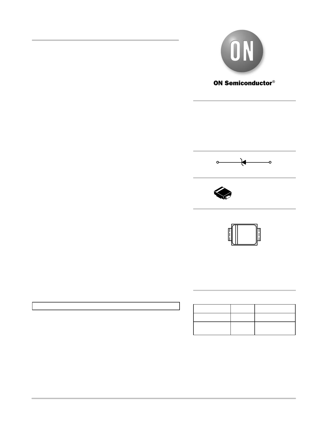
Cathode
Anode
SMB
CASE 403A
PLASTIC
MARKING DIAGRAM
AYWW
xx G
G
A = Assembly Location
Y = Year
WW = Work Week
xx = Device Code (Refer to page 3)
G = Pb−Free Package
(Note: Microdot may be in either location)
ORDERING INFORMATION
Device
Package
Shipping†
P6SMBxxxAT3
SMB 2500/Tape & Reel
P6SMBxxxAT3G SMB 2500/Tape & Reel
(Pb−Free)
†For information on tape and reel specifications,
including part orientation and tape sizes, please
refer to our Tape and Reel Packaging Specifications
Brochure, BRD8011/D.
© Semiconductor Components Industries, LLC, 2007
February, 2007 − Rev. 8
1
Publication Order Number:
P6SMB6.8AT3/D
1 page 
P6SMB6.8AT3 Series
APPLICATION NOTES
RESPONSE TIME
In most applications, the transient suppressor device is
placed in parallel with the equipment or component to be
protected. In this situation, there is a time delay associated
with the capacitance of the device and an overshoot
condition associated with the inductance of the device and
the inductance of the connection method. The capacitive
effect is of minor importance in the parallel protection
scheme because it only produces a time delay in the
transition from the operating voltage to the clamp voltage as
shown in Figure 5.
The inductive effects in the device are due to actual
turn-on time (time required for the device to go from zero
current to full current) and lead inductance. This inductive
effect produces an overshoot in the voltage across the
equipment or component being protected as shown in
Figure 6. Minimizing this overshoot is very important in the
application, since the main purpose for adding a transient
suppressor is to clamp voltage spikes. The SMB series have
a very good response time, typically < 1 ns and negligible
inductance. However, external inductive effects could
produce unacceptable overshoot. Proper circuit layout,
minimum lead lengths and placing the suppressor device as
close as possible to the equipment or components to be
protected will minimize this overshoot.
Some input impedance represented by Zin is essential to
prevent overstress of the protection device. This impedance
should be as high as possible, without restricting the circuit
operation.
DUTY CYCLE DERATING
The data of Figure 1 applies for non-repetitive conditions
and at a lead temperature of 25°C. If the duty cycle increases,
the peak power must be reduced as indicated by the curves
of Figure 7. Average power must be derated as the lead or
ambient temperature rises above 25°C. The average power
derating curve normally given on data sheets may be
normalized and used for this purpose.
At first glance the derating curves of Figure 7 appear to be
in error as the 10 ms pulse has a higher derating factor than
the 10 ms pulse. However, when the derating factor for a
given pulse of Figure 7 is multiplied by the peak power value
of Figure 1 for the same pulse, the results follow the
expected trend.
http://onsemi.com
5
5 Page | ||
| Páginas | Total 7 Páginas | |
| PDF Descargar | [ Datasheet P6SMB6.8AT3.PDF ] | |
Hoja de datos destacado
| Número de pieza | Descripción | Fabricantes |
| P6SMB6.8AT3 | 600 Watt Peak Power Zener Transient Voltage Suppressors | ON Semiconductor |
| Número de pieza | Descripción | Fabricantes |
| SLA6805M | High Voltage 3 phase Motor Driver IC. |
Sanken |
| SDC1742 | 12- and 14-Bit Hybrid Synchro / Resolver-to-Digital Converters. |
Analog Devices |
|
DataSheet.es es una pagina web que funciona como un repositorio de manuales o hoja de datos de muchos de los productos más populares, |
| DataSheet.es | 2020 | Privacy Policy | Contacto | Buscar |