|
|
|
PDF AD8354 Data sheet ( Hoja de datos )
| Número de pieza | AD8354 | |
| Descripción | RF Gain Block | |
| Fabricantes | Analog Devices | |
| Logotipo | ||
1. AD8354 Hay una vista previa y un enlace de descarga de AD8354 (archivo pdf) en la parte inferior de esta página. Total 17 Páginas | ||
|
No Preview Available !
Data Sheet
FEATURES
Fixed gain of 20 dB
Operational frequency of 1 MHz to 2.7 GHz
Linear output power up to 4 dBm
Input/output internally matched to 50 Ω
Temperature and power supply stable
Noise figure: 4.2 dB
Power supply: 3 V or 5 V
APPLICATIONS
VCO buffers
General Tx/Rx amplification
Power amplifier predrivers
Low power antenna drivers
GENERAL DESCRIPTION
The AD8354 is a broadband, fixed-gain, linear amplifier that
operates at frequencies from 1 MHz up to 2.7 GHz. It is
intended for use in a wide variety of wireless devices, including
cellular, broadband, CATV, and LMDS/MMDS applications.
By taking advantage of ADI’s high performance, complementary Si
bipolar process, these gain blocks provide excellent stability
over process, temperature, and power supply. This amplifier is
single-ended and internally matched to 50 Ω with a return loss
of greater than 10 dB over the full operating frequency range.
The AD8354 provides linear output power of nearly 4.3 dBm
with 20 dB of gain at 900 MHz when biased at 3 V and an
external RF choke is connected between the power supply and
the output pin. The dc supply current is 24 mA. At 900 MHz,
the output third-order intercept (OIP3) is greater than 18 dBm;
at 2.7 GHz, the OIP3 is 14 dBm.
1 MHz to 2.7 GHz
RF Gain Block
AD8354
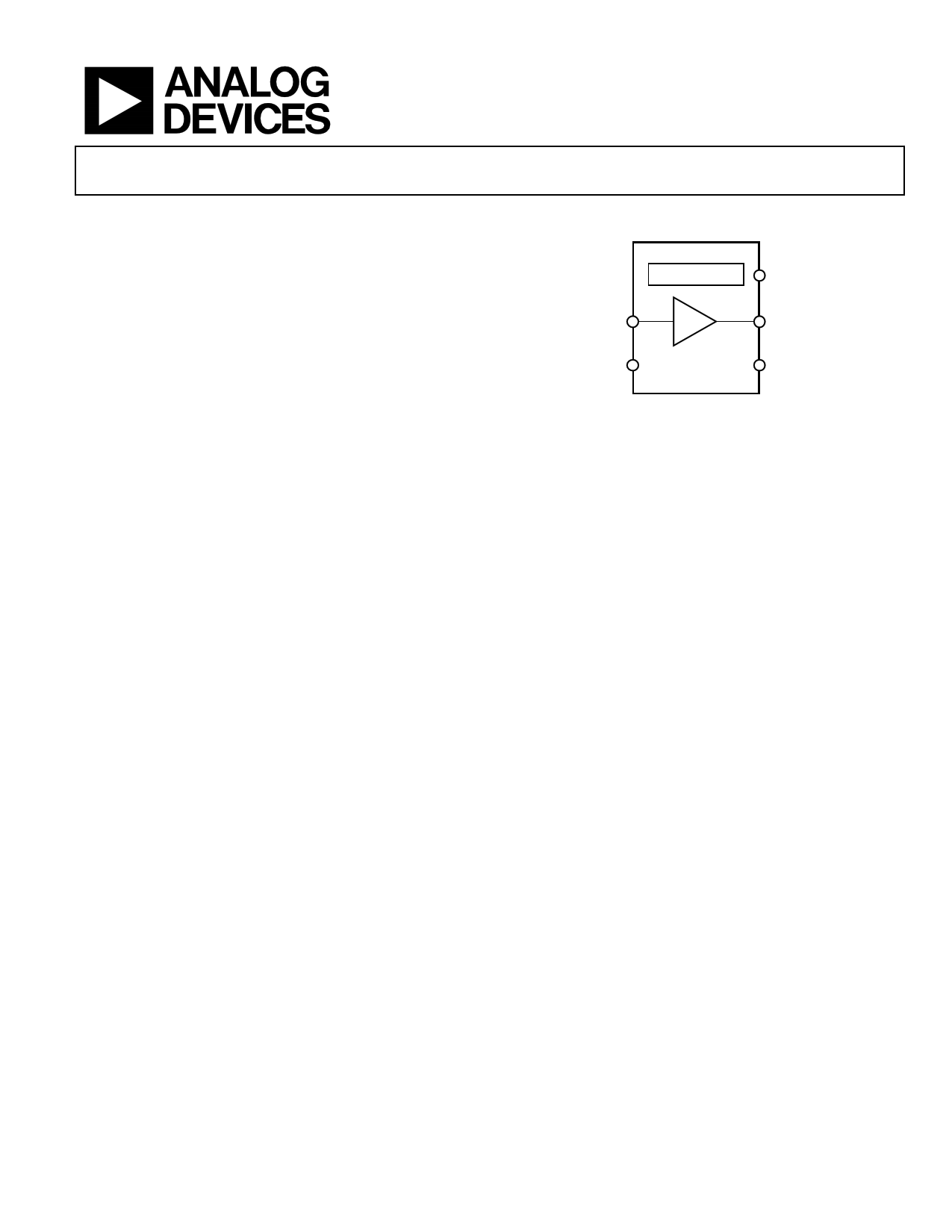
FUNCTIONAL BLOCK DIAGRAM
BIAS AND VREF
VPOS
INPT
COM1
AD8354
Figure 1.
VOUT
COM2
The noise figure is 4.2 dB at 900 MHz. The reverse isolation
(S12) is −33 dB at 900 MHz.
The AD8354 can also operate with a 5 V power supply; in
which case, no external inductor is required. Under these
conditions, the AD8354 delivers 4.88 dBm with 20 dB of gain
at 900 MHz. The dc supply current is 26 mA. At 900 MHz, the
OIP3 is greater than 19 dBm; at 2.7 GHz, the OIP3 is 15 dBm.
The noise figure is 4.4 dB at 900 MHz. The reverse isolation
(S12) is −33 dB.
The AD8354 is fabricated on ADI’s proprietary, high performance,
25 GHz, Si complementary, bipolar IC process. The AD8354 is
available in a chip scale package that uses an exposed paddle for
excellent thermal impedance and low impedance electrical
connection to ground. It operates over a −40°C to +85°C
temperature range, and an evaluation board is also available.
Rev. E
Document Feedback
Information furnished by Analog Devices is believed to be accurate and reliable. However, no
responsibilityisassumedbyAnalogDevices for itsuse,nor foranyinfringementsofpatentsor other
rights of third parties that may result from its use. Specifications subject to change without notice. No
license is granted by implication or otherwise under any patent or patent rights of Analog Devices.
Trademarks and registered trademarks are the property of their respective owners.
One Technology Way, P.O. Box 9106, Norwood, MA 02062-9106, U.S.A.
Tel: 781.329.4700 ©2002–2013 Analog Devices, Inc. All rights reserved.
Technical Support
www.analog.com
1 page 
AD8354
Data Sheet
VS = 5 V, TA = 25°C, no external inductor between VOUT and VPOS, ZO = 50 Ω, unless otherwise noted.
Table 2.
Parameter
Conditions
Min
OVERALL FUNCTION
Frequency Range
1
Gain f = 900 MHz
f = 1.9 GHz
Delta Gain
Gain Supply Sensitivity
f = 2.7 GHz
f = 900 MHz, −40°C ≤ TA ≤ +85°C
f = 1.9 GHz, −40°C ≤ TA ≤ +85°C
f = 2.7 GHz, −40°C ≤ TA ≤ +85°C
VPOS ± 10%, f = 900 MHz
f = 1.9 GHz
Reverse Isolation (S12)
f = 2.7 GHz
f = 900 MHz
f = 1.9 GHz
f = 2.7 GHz
RF INPUT INTERFACE
Input Return Loss
Pin INPT
f = 900 MHz
f = 1.9 GHz
f = 2.7 GHz
RF OUTPUT INTERFACE
Output Compression Point
Pin VOUT
f = 900 MHz
f = 1.9 GHz
f = 2.7 GHz
Delta Compression Point
Output Return Loss
f = 900 MHz, −40°C ≤ TA ≤ +85°C
f = 1.9 GHz, −40°C ≤ TA ≤ +85°C
f = 2.7 GHz, −40°C ≤ TA ≤ +85°C
f = 900 MHz
f = 1.9 GHz
f = 2.7 GHz
DISTORTION/NOISE
Output Third-Order Intercept
Output Second-Order Intercept
Noise Figure
f = 900 MHz, ∆f = 50 MHz, PIN = −30 dBm
f = 1.9 GHz, ∆f = 50 MHz, PIN = −30 dBm
f = 2.7 GHz, ∆f = 50 MHz, PIN = −30 dBm
f = 900 MHz, ∆f = 1 MHz, PIN = −28 dBm
f = 900 MHz
f = 1.9 GHz
f = 2.7 GHz
POWER INTERFACE
Supply Voltage
Total Supply Current
Supply Voltage Sensitivity
Temperature Sensitivity
Pin VPOS
TA = 27°C
−40°C ≤ TA ≤ +85°C
4.5
17
Typ
19.5
18.7
17.3
−0.93
−0.99
−1.21
0.32
0.21
0.08
−33.5
−37.6
−32.9
24.4
23.9
13.5
4.8
4.6
3.6
0.37
−0.14
−0.05
23.7
22.5
17.6
19.3
17.3
15.3
28.7
4.4
5
5.6
5
25
4
28
Max
2700
5.5
34
Unit
MHz
dB
dB
dB
dB
dB
dB
dB/V
dB/V
dB/V
dB
dB
dB
dB
dB
dB
dBm
dBm
dBm
dB
dB
dB
dB
dB
dB
dBm
dBm
dBm
dBm
dB
dB
dB
V
mA
mA/V
µA/°C
Rev. E | Page 4 of 16
5 Page 
AD8354
Data Sheet
25
GAIN AT 5.5V
20
15 GAIN AT 5.0V GAIN AT 4.5V
10
5
25
GAIN AT –�40°C
20
15
GAIN AT +�25°C
10
GAIN AT +85°C
5
0
0
500
1000
1500
2000
2500
3000
FREQUENCY (MHz)
Figure 21. Gain vs. Frequency, VS = 4.5 V, 5 V, and 5.5 V, TA = 25°C
0
–5
–10
–15
–20
–25 S12 AT 4.5V
S12 AT 5.0V
–30
S12 AT 5.5V
–35
–40
0
500
1000
1500
2000
2500
3000
FREQUENCY (MHz)
Figure 22. Reverse Isolation vs. Frequency, VS = 4.5 V, 5 V, and 5.5 V, TA = 25°C
7
6 P1dB AT 5.5V
5
4
3 P1dB AT 5.0V
2
P1dB AT 4.5V
1
0
0
500
1000
1500
2000
2500
3000
FREQUENCY (MHz)
Figure 23. P1dB vs. Frequency, VS = 4.5 V, 5 V, and 5.5 V, TA = 25°C
0
0
500
1000
1500
2000
2500
3000
FREQUENCY (MHz)
Figure 24. Gain vs. Frequency, VS = 5 V, TA = −40°C, +25°C, and +85°C
0
–5
–10
–15
–20
–25 S12 AT –40°C
S12 AT +85°C S12 AT +25°C
–30
–35
–40
0
500
1000
1500
2000
2500 3000
FREQUENCY (MHz)
Figure 25. Reverse Isolation vs. Frequency, VS = 5 V, TA = −40°C, +25°C, and +85°C
6
P1dB AT +85°C
5
P1dB AT –40°C
4
P1dB AT +25°C
3
2
1
0
0
500
1000
1500
2000
2500
3000
FREQUENCY (MHz)
Figure 26. P1dB vs. Frequency, VS = 5 V, TA = –40°C, +25°C, and +85°C
Rev. E | Page 10 of 16
11 Page | ||
| Páginas | Total 17 Páginas | |
| PDF Descargar | [ Datasheet AD8354.PDF ] | |
Hoja de datos destacado
| Número de pieza | Descripción | Fabricantes |
| AD835 | 4-Quadrant Multiplier | Analog Devices |
| AD8350 | Low Distortion 1.0 GHz Differential Amplifier | Analog Devices |
| AD8351 | Low Distortion Differential RF/IF Amplifier | Analog Devices |
| AD8352 | 2 GHz Ultra Low Distortion Differential RF/IF Amplifier | Analog Devices |
| Número de pieza | Descripción | Fabricantes |
| SLA6805M | High Voltage 3 phase Motor Driver IC. |
Sanken |
| SDC1742 | 12- and 14-Bit Hybrid Synchro / Resolver-to-Digital Converters. |
Analog Devices |
|
DataSheet.es es una pagina web que funciona como un repositorio de manuales o hoja de datos de muchos de los productos más populares, |
| DataSheet.es | 2020 | Privacy Policy | Contacto | Buscar |