|
|
|
PDF WM8196 Data sheet ( Hoja de datos )
| Número de pieza | WM8196 | |
| Descripción | (8 + 8) Bit Output 16-bit CIS/CCD AFE/Digitiser | |
| Fabricantes | Wolfson Microelectronics | |
| Logotipo | ||
Hay una vista previa y un enlace de descarga de WM8196 (archivo pdf) en la parte inferior de esta página. Total 30 Páginas | ||
|
No Preview Available !
w
WM8196
(8 + 8) Bit Output 16-bit CIS/CCD AFE/Digitiser
DESCRIPTION
FEATURES
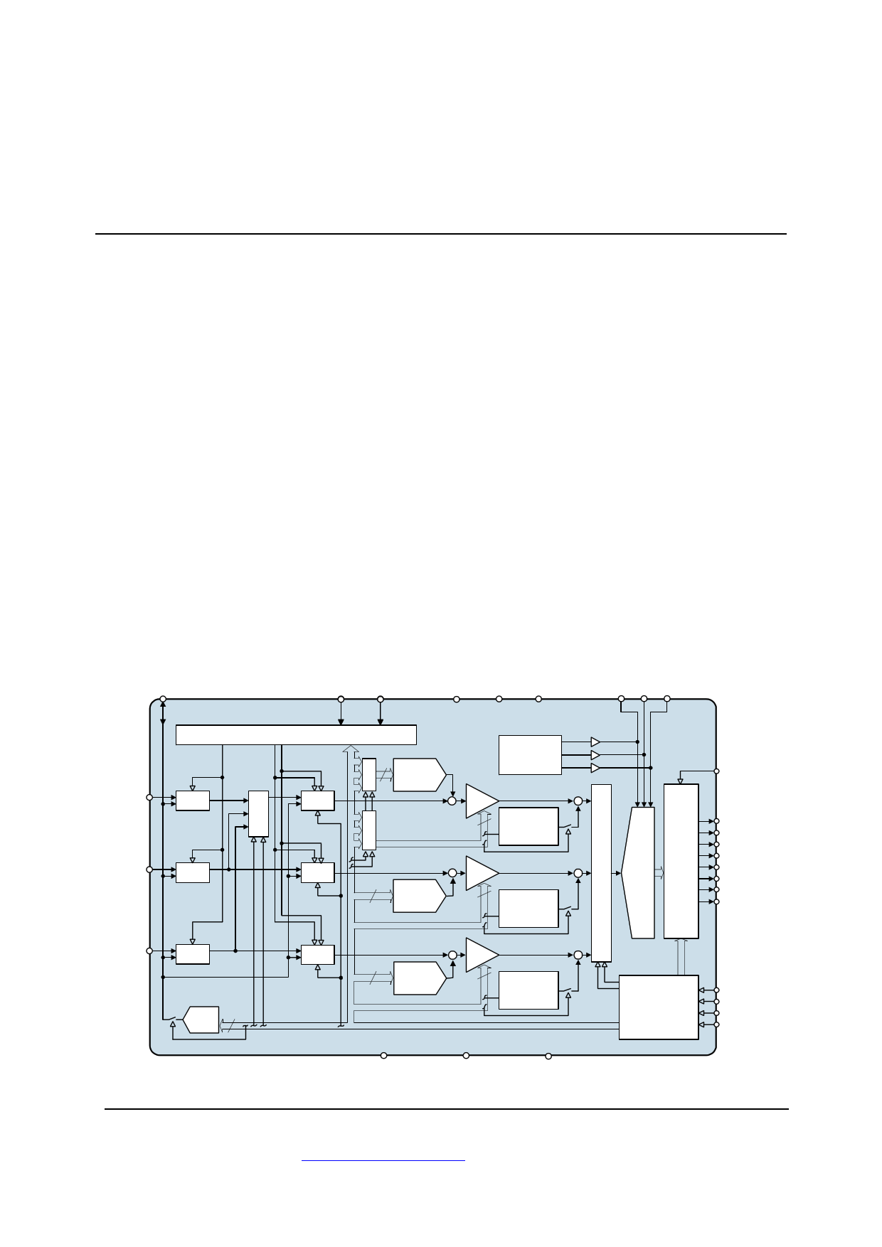
The WM8196 is a 16-bit analogue front end/digitiser IC
which processes and digitises the analogue output signals
from CCD sensors or Contact Image Sensors (CIS) at pixel
sample rates of up to 12MSPS.
• 16-bit ADC
• 12MSPS conversion rate
• Low power – 320mW typical
• 5V single supply or 5V/3.3V dual supply operation
The device includes three analogue signal processing
channels each of which contains Reset Level Clamping,
Correlated Double Sampling and Programmable Gain and
Offset adjust functions. Three multiplexers allow single
channel processing. The output from each of these
channels is time multiplexed into a single high-speed 16-bit
• Single or 3 channel operation
• Correlated double sampling
• Programmable gain (8-bit resolution)
• Programmable offset adjust (8-bit resolution)
• Programmable clamp voltage
Analogue to Digital Converter. The digital output data is
available in 8 or 4-bit wide multiplexed format.
• 8 or 4-bit wide multiplexed data output formats
• Internally generated voltage references
An internal 4-bit DAC is supplied for internal reference level
• 28-lead SSOP package
generation. This may be used during CDS to reference CIS
signals or during Reset Level Clamping to clamp CCD
signals. An external reference level may also be supplied.
ADC references are generated internally, ensuring optimum
performance from the device.
• Serial control interface
APPLICATIONS
• Flatbed and sheetfeed scanners
Using an analogue supply voltage of 5V and a digital
interface supply of either 5V or 3.3V, the WM8196 typically
• USB compatible scanners
• Multi-function peripherals
only consumes 300mW when operating from a single
• High-performance CCD sensor interface
5V supply.
www.DataSheet4U.com
BLOCK DIAGRAM
VRLC/VBIAS
VSMP MCLK
AVDD DVDD1 DVDD2
VRT VRX VRB
RINP
GINP
CL
RLC
RLC
RS VS
M
U
X
TIMING CONTROL
w
WM8196
CDS
RM
GU
X
B
8
OFFSET
DAC
VREF/BIAS
+ PGA
RM
GU
X
B
I/P SIGNAL
8 POLARITY
ADJUST
CDS
+ PGA
8 OFFSET
DAC
8 I/P SIGNAL
POLARITY
ADJUST
+
M
+U
X
16-
BIT
ADC
DATA
I/O
PORT
OEB
OP[0]
OP[1]
OP[2]
OP[3]
OP[4]
OP[5]
OP[6]
OP[7]/SDO
BINP
RLC
RLC 4
DAC
CDS
+ PGA
+
8 OFFSET
DAC
8 I/P SIGNAL
POLARITY
ADJUST
CONFIGURABLE
SERIAL
CONTROL
INTERFACE
SEN
SCK
SDI
RLC/ACYC
AGND1
AGND2
DGND
WOLFSON MICROELECTRONICS plc
To receive regular email updates, sign up at http://www.wolfsonmicro.com/enews/
Production Data, March 2007, Rev 4.3
Copyright ©2007 Wolfson Microelectronics plc
1 page 
WM8196
Production Data
ABSOLUTE MAXIMUM RATINGS
Absolute Maximum Ratings are stress ratings only. Permanent damage to the device may be caused by continuously operating at
or beyond these limits. Device functional operating limits and guaranteed performance specifications are given under Electrical
Characteristics at the test conditions specified.
ESD Sensitive Device. This device is manufactured on a CMOS process. It is therefore generically susceptible
to damage from excessive static voltages. Proper ESD precautions must be taken during handling and storage
of this device.
Wolfson tests its package types according to IPC/JEDEC J-STD-020B for Moisture Sensitivity to determine acceptable storage
conditions prior to surface mount assembly. These levels are:
MSL1 = unlimited floor life at <30°C / 85% Relative Humidity. Not normally stored in moisture barrier bag.
MSL2 = out of bag storage for 1 year at <30°C / 60% Relative Humidity. Supplied in moisture barrier bag.
MSL3 = out of bag storage for 168 hours at <30°C / 60% Relative Humidity. Supplied in moisture barrier bag.
The Moisture Sensitivity Level for each package type is specified in Ordering Information.
CONDITION
MIN MAX
Analogue supply voltage: AVDD
GND - 0.3V
GND + 7V
Digital supply voltages: DVDD1 − 2
GND - 0.3V
GND + 7V
Digital ground: DGND
GND - 0.3V
GND + 0.3V
Analogue grounds: AGND1 − 2
GND - 0.3V
GND + 0.3V
Digital inputs, digital outputs and digital I/O pins
GND - 0.3V
DVDD2 + 0.3V
Analogue inputs (RINP, GINP, BINP)
GND - 0.3V
AVDD + 0.3V
Other pins
GND - 0.3V
AVDD + 0.3V
Operating temperature range: TA
Storage temperature prior to soldering
Storage temperature after soldering
0°C
-65°C
+70°C
30°C max / 85% RH max
+150°C
Notes:
1. GND denotes the voltage of any ground pin.
2. AGND1, AGND2 and DGND pins are intended to be operated at the same potential. Differential voltages
between these pins will degrade performance.
RECOMMENDED OPERATING CONDITIONS
CONDITION
SYMBOL
MIN
TYP
MAX
UNITS
Operating temperature range
TA 0
70 °C
Analogue supply voltage
AVDD
4.75
5.0
5.25
V
Digital core supply voltage
DVDD1
4.75
5.0
5.25
V
Digital I/O supply voltage
5V I/O
DVDD2
4.75
5.0
5.25
3.3V I/O
DVDD2
2.97
3.3
3.63
V
V
THERMAL PERFORMANCE
PARAMETER
Performance
Thermal resistance – junction to
case
Thermal resistance – junction to
ambient
SYMBOL TEST CONDITIONS
RθJC
RθJA
Tambient = 25°C
MIN
TYP
23.9
67.1
Notes:
1. Figures given are for package mounted on 4-layer FR4 according to JESD51-5 and JESD51-7.
w
MAX
UNIT
°C/W
°C/W
PD Rev 4.3 March 2007
5
5 Page 
WM8196
INTERNAL POWER ON RESET CIRCUIT
Production Data
Figure 6 Internal Power On Reset Circuit Schematic
The WM8196 includes an internal Power-On-Reset Circuit, as shown in Figure 6, which is used to
reset the digital logic into a default state after power up. The POR circuit is powered from AVDD and
monitors DVDD1. It asserts PORB low if AVDD or DVDD1 is below a minimum threshold.
The power supplies can be brought up in any order but is important that either AVDD is brought up
and is stable before DVDD comes up or vice versa as shown in Figure 7 and Figure 8.
Figure 7 Typical Power up Sequence where AVDD is Powered before DVDD1
Figure 7 shows a typical power-up sequence where AVDD is powered up first. When AVDD rises
above the minimum threshold, Vpora, there is enough voltage for the circuit to guarantee PORB is
asserted low and the chip is held in reset. In this condition, all writes to the control interface are
ignored. Now AVDD is at full supply level. Next DVDD1 rises to Vpord_on and PORB is released
high and all registers are in their default state and writes to the control interface may take place.
On power down, where AVDD falls first, PORB is asserted low whenever AVDD drops below the
minimum threshold Vpora_off.
w
PD Rev 4.3 March 2007
11
11 Page | ||
| Páginas | Total 30 Páginas | |
| PDF Descargar | [ Datasheet WM8196.PDF ] | |
Hoja de datos destacado
| Número de pieza | Descripción | Fabricantes |
| WM8190 | (8+6) Bit Output 14-bit CIS/CCD AFE/Digitiser | Wolfson Microelectronics plc |
| WM8191 | 14-bit 6MSPS CIS/CCD Analogue Front End/Digitiser | Wolfson Microelectronics plc |
| WM8192 | (8+8) Bit Output 16-bit CIS/CCD AFE/Digitiser | Wolfson Microelectronics plc |
| WM8195 | 14-bit 12MSPS CIS/CCD Analogue Front End/Digitiser | Wolfson Microelectronics |
| Número de pieza | Descripción | Fabricantes |
| SLA6805M | High Voltage 3 phase Motor Driver IC. |
Sanken |
| SDC1742 | 12- and 14-Bit Hybrid Synchro / Resolver-to-Digital Converters. |
Analog Devices |
|
DataSheet.es es una pagina web que funciona como un repositorio de manuales o hoja de datos de muchos de los productos más populares, |
| DataSheet.es | 2020 | Privacy Policy | Contacto | Buscar |