|
|
|
PDF C3199 Data sheet ( Hoja de datos )
| Número de pieza | C3199 | |
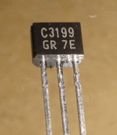
| Descripción | NPN Transistor - 2SC3199 | |
| Fabricantes | ETC | |
| Logotipo | ||
 1. 150mA, NPN Transistor - KEC Hay una vista previa y un enlace de descarga de C3199 (archivo pdf) en la parte inferior de esta página. Total 2 Páginas | ||
|
No Preview Available !
2SC3199 NPN Silicon Epitaxial Planar Transistor
for switching and AF amplifier applications.
The transistor is subdivided into four groups, O,
Y, G and L, according to its DC current gain.
On special request, these transistors can be
manufactured in different pin configurations.
Absolute Maximum Ratings (Ta = 25 OC)
Parameter
Collector Base Voltage
Collector Emitter Voltage
Emitter Base Voltage
Collector Current
Emitter Current
Power Dissipation
Junction Temperature
Storage Temperature Range
1. Emitter 2. Collector 3. Base
TO-92 Plastic Package
Symbol
VCBO
VCEO
VEBO
IC
IE
Ptot
Tj
Tstg
Value
50
50
5
150
-150
400
150
- 55 to + 150
Unit
V
V
V
mA
mA
mW
OC
OC
Characteristics at Ta = 25 OC
Parameter
Symbol Min. Typ. Max. Unit
DC Current Gain
at VCE = 6 V, IC = 2 mA
Current Gain Group O
Y
G
L
hFE
hFE
hFE
hFE
Collector Base Cutoff Current
at VCB = 50 V
ICBO
Emitter Base Cutoff Current
at VEB = 5 V
IEBO
Collector Emitter Saturation Voltage
at IC = 100 mA, IB = 10 mA
VCE(sat)
Transition Frequency
at VCE = 10 V, IC = 1 mA
fT
Collector Output Capacitance
at VCB = 10 V, f = 1 MHz
Cob
Noise Figure
at VCE = 6 V, IC = 0.1 mA, f = 1 KHz, RG = 10 KΩ
NF
70
120
200
350
-
-
-
80
-
-
- 140 -
- 240 -
- 400 -
- 700 -
- 0.1 µA
- 0.1 µA
0.1 0.25
V
- - MHz
2 3.5 pF
1 10 dB
Page 1 of 2
7/15/2011
1 page | ||

| Páginas | Total 2 Páginas | |
| PDF Descargar | [ Datasheet C3199.PDF ] | |
Hoja de datos destacado
| Número de pieza | Descripción | Fabricantes |
| C3192 | NPN SIlicon | Jing Hi-Tech |
| C3192 | NPN Transistor | TIP |
| C3194 | NPN Transistor | TIP |
| C3195 | NPN silicon | FGX |
| Número de pieza | Descripción | Fabricantes |
| SLA6805M | High Voltage 3 phase Motor Driver IC. |
Sanken |
| SDC1742 | 12- and 14-Bit Hybrid Synchro / Resolver-to-Digital Converters. |
Analog Devices |
|
DataSheet.es es una pagina web que funciona como un repositorio de manuales o hoja de datos de muchos de los productos más populares, |
| DataSheet.es | 2020 | Privacy Policy | Contacto | Buscar |