|
|
|
PDF DS1340 Data sheet ( Hoja de datos )
| Número de pieza | DS1340 | |
| Descripción | I2C RTC | |
| Fabricantes | Maxim Integrated Products | |
| Logotipo | ||
Hay una vista previa y un enlace de descarga de DS1340 (archivo pdf) en la parte inferior de esta página. Total 13 Páginas | ||
|
No Preview Available !
Rev 2; 12/04
www.DataSheet4U.com
I2C RTC with Trickle Charger
General Description
The DS1340 is a real-time clock (RTC)/calendar that is
pin compatible and functionally equivalent to the ST
M41T00, including the software clock calibration. The
device additionally provides trickle-charge capability
on the VBACKUP pin, a lower timekeeping voltage, and
an oscillator STOP flag. Block access of the register
map is identical to the ST device. Two additional regis-
ters, which are accessed individually, are required for
the trickle charger and flag. The clock/calendar pro-
vides seconds, minutes, hours, day, date, month, and
year information. A built-in power-sense circuit detects
power failures and automatically switches to the back-
up supply. The device is programmed serially through
an I2CTM bidirectional bus.
Portable Instruments
Point-of-Sale Equipment
Medical Equipment
Telecommunications
Applications
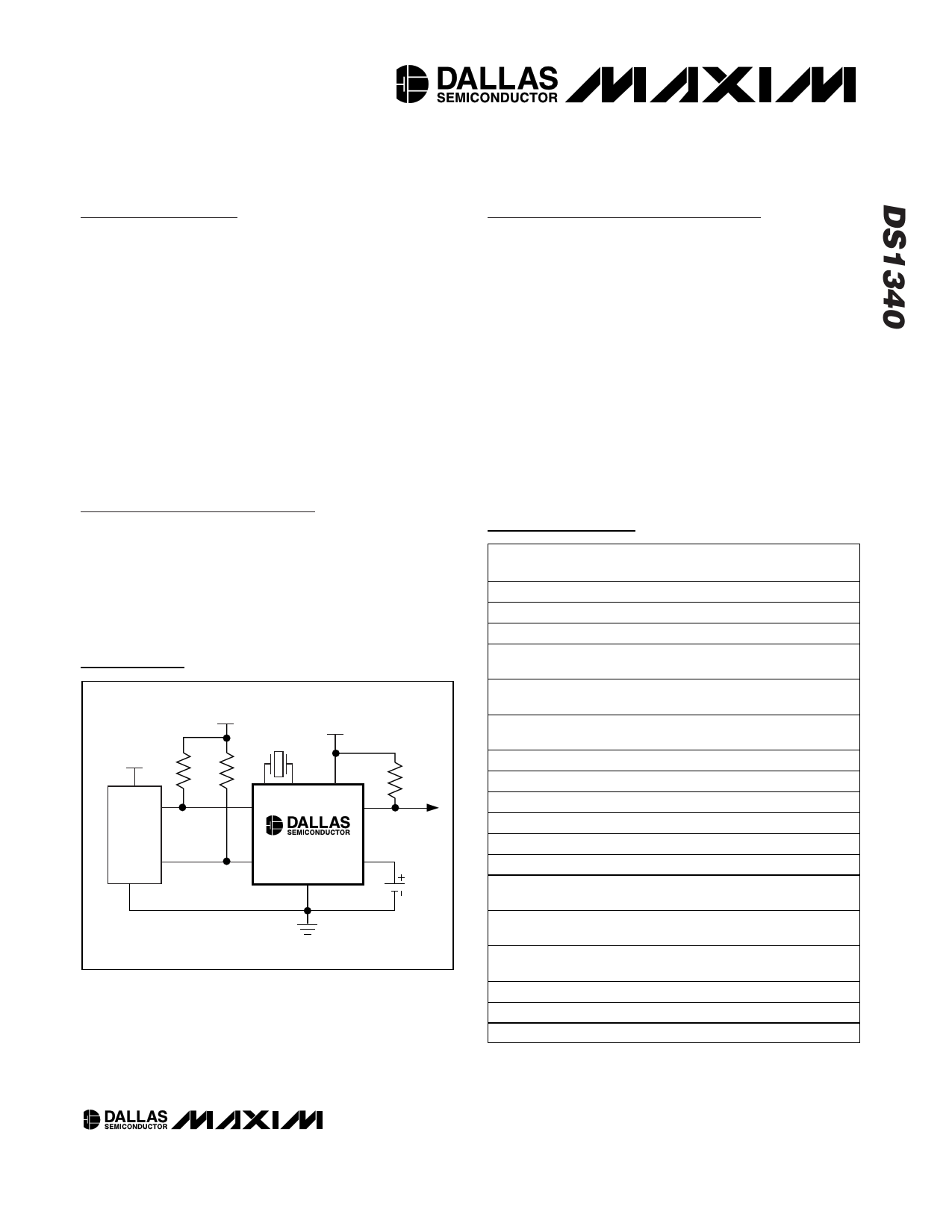
Typical Operating Circuit
VCC RPU
VCC
CRYSTAL
RPU
1
X1
6 SCL
2
X2
VCC
8
VCC 7
FT/OUT
CPU
RPU = tR / CB
5 SDA
DS1340
3
VBACKUP
GND
4
I2C is a trademark of Philips Corp. Purchase of I2C compo-
nents from Maxim Integrated Products, Inc., or one of its subli-
censed Associated Companies, conveys a license under the
Philips I2C Patent Rights to use these components in an I2C
system, provided that the system conforms to the I2C Standard
Specification as defined by Philips.
Features
♦ Enhanced Second Source for the ST M41T00
♦ Available in a Surface-Mount Package with an
Integrated Crystal (DS1340C)
♦ Fast (400kHz) I2C Interface
♦ Software Clock Calibration
♦ RTC Counts Seconds, Minutes, Hours, Day, Date,
Month, and Year
♦ Automatic Power-Fail Detect and Switch Circuitry
♦ Trickle-Charge Capability
♦ Low Timekeeping Voltage Down to 1.3V
♦ Three Operating Voltage Ranges (1.8V, 3V, and 3.3V)
♦ Oscillator Stop Flag
♦ Available in 8-Pin µSOP or SO Packages
♦ Underwriters Laboratory (UL) Recognized
Ordering Information
PART
TEMP RANGE
PIN-PACKAGE
TOP
MARK
DS1340Z-18 -40°C to +85°C 8 SO (0.150in) D1340-18
DS1340Z-3 -40°C to +85°C 8 SO (0.150in) DS1340-3
DS1340Z-33 -40°C to +85°C 8 SO (0.150in) D1340-33
DS1340U-18 -40°C to +85°C 8 µSOP
DS1340U-3 -40°C to +85°C 8 µSOP
1340
A1-18
1340
A1-3
DS1340U-33 -40°C to +85°C 8 µSOP
1340
A1-33
DS1340C-18 -40°C to +85°C 16 SO
1340C-18
DS1340C-3 -40°C to +85°C 16 SO
1340C-3
DS1340C-33 -40°C to +85°C 16 SO
1340C-33
DS1340Z-18+ -40°C to +85°C 8 SO (0.150in) D1340-18
DS1340Z-3+ -40°C to +85°C 8 SO (0.150in) DS1340-3
DS1340Z-33+ -40°C to +85°C 8 SO (0.150in) D1340-33
DS1340U-18+ -40°C to +85°C 8 µSOP
1340
A1-18
DS1340U-3+ -40°C to +85°C 8 µSOP
1340
A1-3
DS1340U-33+ -40°C to +85°C 8 µSOP
1340
A1-33
DS1340C-18+ -40°C to +85°C 16 SO
1340C-18
DS1340C-3+ -40°C to +85°C 16 SO
1340C-3
DS1340C-33+ -40°C to +85°C 16 SO
1340C-33
Note: A "+" in the part number and a "+" anywhere on the top
mark indicates a lead-free device.
Pin Configurations appear at end of data sheet.
______________________________________________ Maxim Integrated Products 1
For pricing, delivery, and ordering information, please contact Maxim/Dallas Direct! at
1-888-629-4642, or visit Maxim’s website at www.maxim-ic.com.
1 page 
I2C RTC with Trickle Charger
VCC
VPF(MAX)
VPF(MIN)
RST
VPF
tF
VPF
tR
tRPU
tRST
INPUTS
RECOGNIZED
DON'T CARE
RECOGNIZED
OUTPUTS
VALID
HIGH-Z
VALID
Figure 2. Power-Up/Power-Down Timing
(VCC = +3.3V, TA = +25°C, unless otherwise noted.)
Typical Operating Characteristics
ICCSA vs. VCC FT = 0
250
ICCS vs. VCC FT = 0
150
IBACKUP1 (FT = 0) vs. VBACKUP
850
800
200
125
-3.3V 750
100 700
150 -3.0V
650
75 -1.8V
600
100
50 550
50
500
25
450
0
1.0 1.5 2.0 2.5 3.0 3.5 4.0 4.5 5.0 5.5
VCC (V)
0
1.0 1.5 2.0 2.5 3.0 3.5 4.0 4.5 5.0 5.5
VCC (V)
400
1.0 1.5 2.0 2.5 3.0 3.5 4.0 4.5 5.0 5.5
VBACKUP (V)
IBACKUP2 (FT = 1) vs. VBACKUP
850
800
750
700
650
600
550
500
450
400
1.0 1.5 2.0 2.5 3.0 3.5 4.0 4.5 5.0 5.5
VBACKUP (V)
IBACKUP3 vs. TEMPERATURE
850 VBACKUP = 3.0V
800
750
700
650
600
550
500
-40 -20
0 20 40 60
TEMPERATURE (°C)
80
512.0000
FT vs. VBACKUP
511.9995
511.9990
511.9985
511.9980
511.9975
511.9970
511.9965
511.9960
1.0 1.5 2.0 2.5 3.0 3.5 4.0 4.5 5.0 5.5
VBACKUP (V)
_____________________________________________________________________ 5
5 Page 
I2C RTC with Trickle Charger
<SLAVE
<WORD
ADDRESS> ADDRESS (n)> <DATA (n)> <DATA (n + 1)> <DATA (n + X)>
S 1101000 0 A XXXXXXXX A XXXXXXXX A XXXXXXXX A XXXXXXXX A P
S — START
A — ACKNOWLEDGE
P — STOP
DATA TRANSFERRED
(X + 1 BYTES + ACKNOWLEDGE)
R/W — READ/WRITE OR DIRECTION BIT ADDRESS = D0H
Figure 8. Slave Receiver Mode (Write Mode)
Accordingly, the following bus conditions have been
defined:
Bus not busy: Both data and clock lines remain
high.
START data transfer: A change in the data line’s
state from high to low, while the clock line is high,
defines a START condition.
STOP data transfer: A change in the data line’s
state from low to high, while the clock line is high,
defines a STOP condition.
Data valid: The data line’s state represents valid
data when, after a START condition, the data line is
stable for the duration of the high period of the
clock signal. The data on the line must be changed
during the low period of the clock signal. There is
one clock pulse per bit of data.
Each data transfer is initiated with a START condi-
tion and terminated with a STOP condition. The
number of data bytes transferred between the
START and STOP conditions is not limited, and is
determined by the master device. The information
is transferred byte-wise and each receiver
acknowledges with a ninth bit.
Acknowledge: Each receiving device, when
addressed, is obliged to generate an acknowl-
edge after the reception of each byte. The master
device must generate an extra clock pulse that is
associated with this acknowledge bit.
A device that acknowledges must pull down the
SDA line during the acknowledge clock pulse in
such a way that the SDA line is stable low during
the high period of the acknowledge-related clock
pulse. Setup and hold times must be taken into
account. A master must signal an end of data to
the slave by not generating an acknowledge bit on
the last byte that has been clocked out of the
slave. In this case, the slave must leave the data
line high to enable the master to generate the
STOP condition.
<SLAVE
ADDRESS>
<DATA (n)> <DATA (n + 1)> <DATA (n + 2)> <DATA (n + X)>
S 1101000 1 A XXXXXXXX A XXXXXXXX A XXXXXXXX A XXXXXXXX A P
S — START
A — ACKNOWLEDGE
P — STOP
A — NOT ACKNOWLEDGE
DATA TRANSFERRED
(X + 1 BYTES + ACKNOWLEDGE)
NOTE: LAST DATA BYTE IS FOLLOWED BY
A NOT ACKNOWLEDGE (A) SIGNAL
R/W — READ/WRITE OR DIRECTION BIT ADDRESS = D0H
Figure 9. Slave Transmitter Mode (Read Mode
Figures 8 and 9 detail how data transfer is accom-
plished on the I2C bus. Depending upon the state of
the R/W bit, two types of data transfer are possible:
Data transfer from a master transmitter to a
slave receiver. The first byte transmitted by the
master is the slave address. Next follows a num-
ber of data bytes. The slave returns an acknowl-
edge bit after each received byte.
Data transfer from a slave transmitter to a mas-
ter receiver. The master transmits the first byte (the
slave address). The slave then returns an acknowl-
edge bit. Next follows a number of data bytes trans-
mitted by the slave to the master. The master
returns an acknowledge bit after all received bytes
other than the last byte. At the end of the last
received byte, a not acknowledge is returned.
The master device generates all the serial clock
pulses and the START and STOP conditions. A
transfer is ended with a STOP condition or with a
repeated START condition. Since a repeated
START condition is also the beginning of the next
serial transfer, the bus is not released.
The DS1340 can operate in the following two modes:
Slave Receiver Mode (Write Mode): Serial data
and clock are received through SDA and SCL.
After each byte is received, an acknowledge bit is
transmitted. Start and STOP conditions are recog-
nized as the beginning and end of a serial trans-
fer. Hardware performs address recognition after
reception of the slave address and direction bit.
The slave address byte is the first byte received
after the master generates the START condition.
The slave address byte contains the 7-bit DS1340
address, which is 1101000, followed by the direc-
tion bit (R/W), which is 0 for a write. After receiving
and decoding the slave address byte, the DS1340
outputs an acknowledge on SDA. After the
DS1340 acknowledges the slave address + write
bit, the master transmits a word address to the
DS1340. This sets the register pointer on the
DS1340, with the DS1340 acknowledging the
transfer. The master can then transmit zero or
____________________________________________________________________ 11
11 Page | ||
| Páginas | Total 13 Páginas | |
| PDF Descargar | [ Datasheet DS1340.PDF ] | |
Hoja de datos destacado
| Número de pieza | Descripción | Fabricantes |
| DS1340 | I2C RTC | Maxim Integrated Products |
| DS1341 | (DS1341 / DS1342) Low-Current I2C RTCs | Maxim Integrated Products |
| DS1342 | (DS1341 / DS1342) Low-Current I2C RTCs | Maxim Integrated Products |
| DS1343 | (DS1343 / DS1344) Low-Current SPI/3-Wire RTCs | Maxim Integrated Products |
| Número de pieza | Descripción | Fabricantes |
| SLA6805M | High Voltage 3 phase Motor Driver IC. |
Sanken |
| SDC1742 | 12- and 14-Bit Hybrid Synchro / Resolver-to-Digital Converters. |
Analog Devices |
|
DataSheet.es es una pagina web que funciona como un repositorio de manuales o hoja de datos de muchos de los productos más populares, |
| DataSheet.es | 2020 | Privacy Policy | Contacto | Buscar |