|
|
|
PDF EM4550 Data sheet ( Hoja de datos )
| Número de pieza | EM4550 | |
| Descripción | (EM4450 / EM4550) 1 KBit Read/Write Contactless Identification Device | |
| Fabricantes | EM Microelectronic | |
| Logotipo | ||
Hay una vista previa y un enlace de descarga de EM4550 (archivo pdf) en la parte inferior de esta página. Total 16 Páginas | ||
|
No Preview Available !
www.DataSheet4U.com
EM MICROELECTRONIC - MARIN SA
EM4450
EM4550
1 KBit Read/Write Contactless Identification Device
Description
The EM4450/4550 is a CMOS integrated circuit intended
for use in electronic Read/Write RF Transponders. The
difference between EM4450 and EM4550 is that EM4550
are bumped and has megapads for the two coils. The chip
contains 1 KBit of EEPROM which can be configured by
the user, allowing a write inhibited area, a read protected
area, and a read area output continuously at power on.
The memory can be secured by using the 32 bit password
for all write and read protected operations. The password
can be updated, but never read. The fixed code serial
number and device identification are laser programmed
making every chip unique.
The EM4450/4550 will transmit data to the transceiver by
modulating the amplitude of the electromagnetic field, and
receive data and commands in a similar way. Simple
commands will enable to write EEPROM, to update the
password, to read a specific memory area, and to reset
the logic.
The coil of the tuned circuit is the only external component
required, all remaining functions are integrated in the chip.
Features
1 KBit of EEPROM organized in 32 words of 32 bits
32 bit Device Serial Number (Read Only Laser ROM)
32 bit Device Identification (Read Only Laser ROM)
Power-On-Reset sequence
Power Check for EEPROM write operation
User defined Read Memory Area at Power On
User defined Write Inhibited Memory Area
User defined Read Protected Memory Area
Data Transmission performed by Amplitude Modulation
Two Data Rate Options 2 KBd (Opt64) or 4 KBd (Opt32)
Bit Period = 64 or 32 periods of field frequency
170 pF ± 2% on chip Resonant Capacitor
-40 to +85°C Temperature range
100 to 150 kHz Field Frequency range
On chip Rectifier and Voltage Limiter
No external supply buffer capacitance needed due to
low power consumption
Available in chip form for mass production and PCB and
CID package for samples.
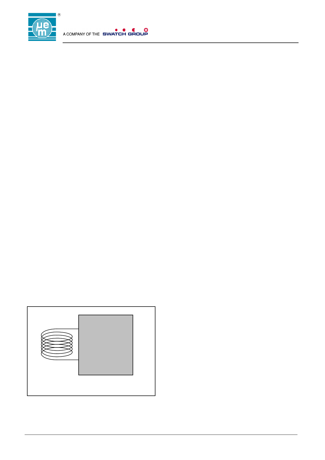
Typical Operating Configuration
Applications
Ticketing
Automotive Immobilizer with rolling code
High Security Hands Free Access Control
Industrial automation with portable database
Manufacturing automation
Prepayment Devices
Coil2
L EM4450
Coil1
Typical value of inductance at 125 kHz is 9.6 mH
Fig.1
Copyright 2003, EM Microelectronic-Marin SA
1
www.emmicroelectronic.com
1 page 
EM4450
EM4550
Memory Organisation
The 1024 bit EEPROM is organised in 32 words of 32 bits. The first three words are assigned to the Password, the
Protection word, and the Control word. In order to write one of these three words, it is necessary to send the valid
password. At fabrication, the EM4450/4550 comes with all bits of the password programmed to a logic "0". The Password
cannot be read out. The memory contains two extra words of Laser ROM. These words are laser programmed during
fabrication for every chip, are unique and cannot be altered.
Memory Map
Word 0
1
3
31
32
33
Bit 0 ------------------------------
PASSWORD
PROTECTION WORD
CONTROL WORD
928 Bits of USER
EEPROM
DEVICE SERIAL NUMBER
DEVICE IDENTIFICATION
Bit 31
EE
EE
EE
EE
Laser
Laser
Control Word
0–7
First Word Read
8 – 15 Last Word Read
16 Password Check On/Off
17 Read After Write On/Off
18 – 31 User available
On means bit set to logic '1'
Off means bit set to logic '0'
Protection Word
0–7
First Word Read Protected
8 – 15
Last Word Read Protected
16 – 23 First Word Write Inhibited
24 – 31 Last Word Write Inhibited
Password
Write Only – No Read Access
Device Identification Word &
Serial Number Word
Laser Programmed – Read only
Fig.5
Standard Read Mode
After a Power-On-Reset and upon completion of a command, the chip will execute the Standard Read Mode, in which it will
send data continuously, word by word from the memory section defined between the First Word Read (FWR) and Last
Word Read (LWR). When the last word is output, the chip will continue with the first word until the transceiver sends a
request. If FWR and LWR are the same, the same word will be sent repetitively. The Listen Window (LIW) is generated
before each word to check if the transceiver is sending data. The LIW has a duration of 320 (160 opt 32) periods of the RF
field. FWR and LWR have to be programmed as valid addresses (FWR ≤ LWR and ≤ 33).
The words sent by the EM4450/4550 comprise 32 data bits and parity bits. The parity bits are not stored in the EEPROM,
but generated while the message is sent as described below. The parity is even for rows and columns, meaning that the
total number of "1's" is even (including the parity bit).
Word organisation (Words 0 to 33)
First bit output
Data
Row Even Parity
D0
D8
D16
D24
PC0
D1 D2
D9 D10
D17 D18
D25 D26
PC1 PC2
D3 D4 D5 D6
D11 D12 D13 D14
D19 D20 D21 D22
D27 D28 D29 D30
PC3 PC4 PC5 PC6
D7
D15
D23
D31
PC7
P0
P1
P2
P3
0
Column Even Partiy
Last bit output
logic '0'
Fig. 6
When a word is read protected, the output will consist of 45 bits set to logic "0". The password has to be used to output
correctly a read protected memory area.
Copyright 2003, EM Microelectronic-Marin SA
5
www.emmicroelectronic.com
5 Page 
EM4450
EM4550
Communication from Transponder to the Transceiver (READ MODE)
The EM4450/4550 modulates the amplitude of the RF field to transmit data to the transceiver. Data are output serially from
the EEPROM and Manchester encoded.
1 bit 64 periods of RF field (Opt64)
32 periods of RF field (Opt32)
1 bit
Data from EEPROM
32 periods (Opt64)
16 periods (Opt32)
1 bit
1 bit
Coded Data Measured on the COIL
Opt64 is the chip option with a bit period corresponding to 64 periods of the RF field
Opt32 is the chip option with a bit period corresponding to 32 periods of the RF field
Fig. 19
The EM4450/4550 uses different patterns to send status information to the transceiver. Their structure can not be confused
with a bit pattern sequence. These patterns are the Listen Window (LIW) to inform the transceiver that data can be
accepted, the Acknowledge (ACK) indicating proper communication and end of EEPROM write, and the No Acknowledge
(NAK) when something is wrong.
The LIW, due to its special structure, can be used to synchronize the transceiver during a read operation. The LIW is sent
before each word, and is sent twice before FWR.
32 32
16 16
LIW
128 64
64 32
64 (Opt64)
32 (Opt32)
32 32
16 16
ACK
96 32
48 16
96 32 (Opt64)
48 16 (Opt32)
32 32
16 16
NAK
96 32 64 32 32 (Opt64)
48 16 32 16 16 (Opt32)
All numbers represent number of periods of RF f ield
Opt64 is the chi p option with a bit period correspondi ng to 64 periods of the RF fiel d
Opt32 is the chi p option with a bit period correspondi ng to 32 periods of the RF fiel d
Fig. 20
Communication from the Transceiver to the Transponder (RECEIVE MODE)
The EM4450/4550 can be switched to the Receive Mode ONLY DURING A LISTEN WINDOW. The Transceiver is
synchronized with the incoming data from the transponder and expects a LIW before each word. During the phase where
the chip has its modulator "ON" (64/32 periods of RF [Opt64/Opt32] ), the transceiver has to send a bit "0". A certain phase
shift in the read path of the transceiver can be accepted due to the fact that when entering Receive Mode, the Transceiver
becomes the Master.
At reception of the first "0", the chip immediately stops the LIW sequence and then expects another bit "0" to activate the
receive mode. Once the EM4450/4550 has received the first bit "0", the transceiver is imposing the timing for
synchronisation.
The EM4450/4550 turns "ON" its modulator at the beginning of each frame of a bit period. To send a logic "1" bit, the
transceiver continues to send clocks without modulation. After half a bit period, the modulation device of the EM4450/4550
is turned "OFF" allowing recharge of the internal supply capacitor. To send a logic "0" bit, the transceiver stops sending
clocks (100% modulation) during the first half of a bit period. The transceiver must not turn "OFF" the field after 7/4 clocks of
the bit period (Opt64/Opt32). The field is stopped for the remaining first half of the bit period, and then turned "ON" again for
the second half of the bit period. The 32rd/16th clock (Opt64/Opt32) defines the end of the bit.
To ensure synchronisation between the transceiver and the transponder, a logic bit set to "0" has to be transmitted at
regular intervals. The RM pattern consists of two bits set to "0" thus allowing initial synchronisation. In addition, the chosen
data structure contains even parity bits which will not allow more than eight consecutive bits set to logic "1" where no
modulation occurs.
Copyright 2003, EM Microelectronic-Marin SA
11
www.emmicroelectronic.com
11 Page | ||
| Páginas | Total 16 Páginas | |
| PDF Descargar | [ Datasheet EM4550.PDF ] | |
Hoja de datos destacado
| Número de pieza | Descripción | Fabricantes |
| EM4550 | (EM4450 / EM4550) 1 KBit Read/Write Contactless Identification Device | EM Microelectronic |
| Número de pieza | Descripción | Fabricantes |
| SLA6805M | High Voltage 3 phase Motor Driver IC. |
Sanken |
| SDC1742 | 12- and 14-Bit Hybrid Synchro / Resolver-to-Digital Converters. |
Analog Devices |
|
DataSheet.es es una pagina web que funciona como un repositorio de manuales o hoja de datos de muchos de los productos más populares, |
| DataSheet.es | 2020 | Privacy Policy | Contacto | Buscar |