|
|
|
PDF WM8152 Data sheet ( Hoja de datos )
| Número de pieza | WM8152 | |
| Descripción | Single Channel 16-bit CIS/CCD AFE | |
| Fabricantes | Wolfson Microelectronics | |
| Logotipo | ||
Hay una vista previa y un enlace de descarga de WM8152 (archivo pdf) en la parte inferior de esta página. Total 26 Páginas | ||
|
No Preview Available !
www.DataSheet4U.com
WM8152
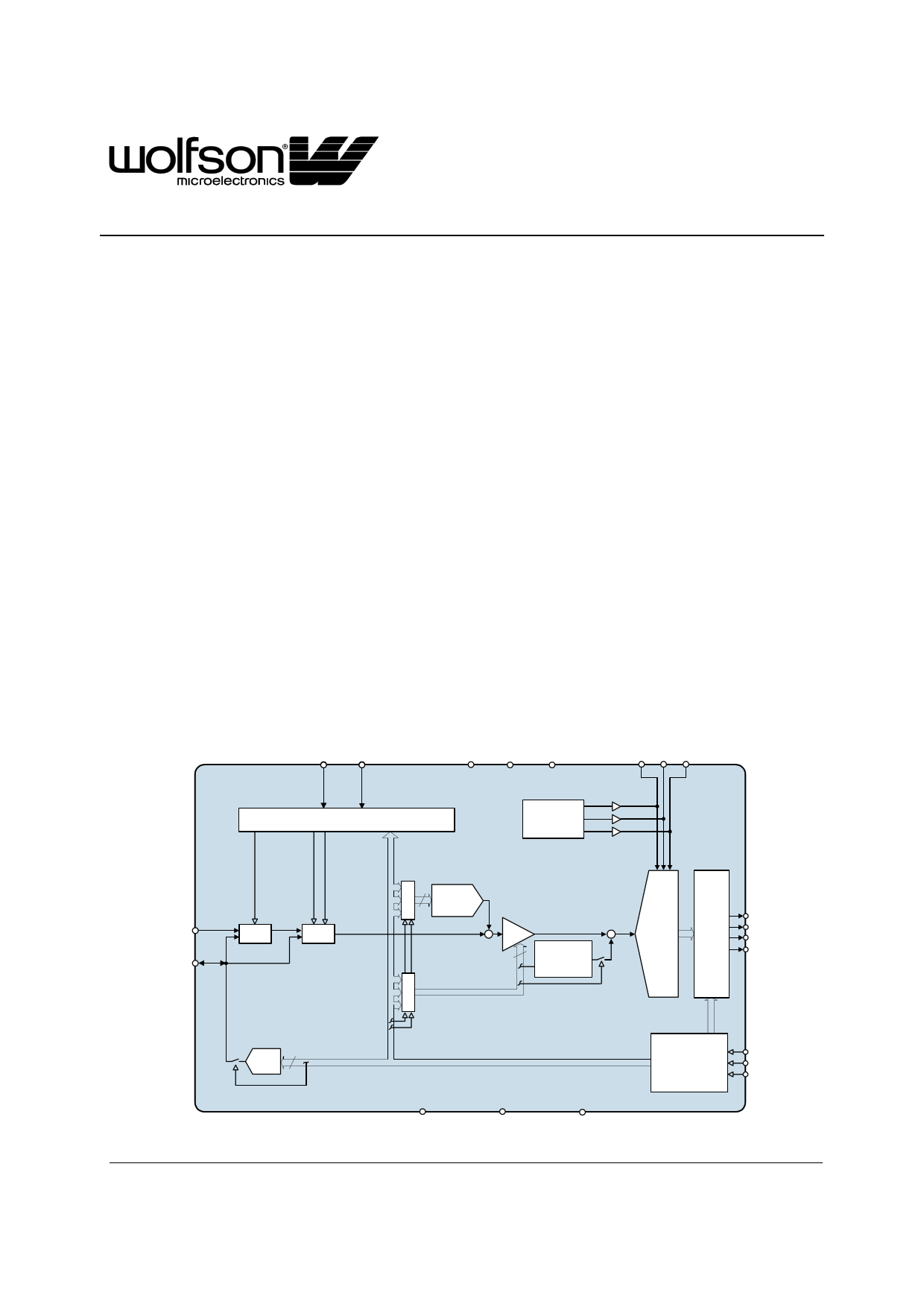
Single Channel 16-bit CIS/CCD AFE with 4-bit Wide Output
DESCRIPTION
The WM8152 is a 16-bit analogue front end/digitiser IC
which processes and digitises the analogue output signals
from CCD sensors or Contact Image Sensors (CIS) at pixel
sample rates of up to 12MSPS.
The device includes a complete analogue signal processing
channel containing Reset Level Clamping, Correlated
Double Sampling, Programmable Gain and Offset adjust
functions. Internal multiplexers allow fast switching of offset
and gain for line-by-line colour processing. The output from
this channel is time multiplexed into a high-speed 16-bit
Analogue to Digital Converter. The digital output data is
available in 4-bit wide multiplexed format.
An internal 4-bit DAC is supplied for internal reference level
generation. This may be used to reference CIS signals or
during Reset Level Clamping to clamp CCD signals. An
external reference level may also be supplied. ADC
references are generated internally, ensuring optimum
performance from the device.
Using an analogue supply voltage of 5V, a digital core
voltage of 5V, and a digital interface supply of either 5V or
3.3V, the WM8152 typically only consumes 225mW when
operating from a single 5V supply.
BLOCK DIAGRAM
FEATURES
• 16-bit ADC
• 12MSPS conversion rate
• Low power - 225mW typical
• 5V single supply or 5V/3.3V dual supply operation
• Single channel operation
• Correlated double sampling
• Programmable gain (8-bit resolution)
• Programmable offset adjust (8-bit resolution)
• Programmable clamp voltage
• 4-bit wide multiplexed data output format
• Internally generated voltage references
• 20-pin SSOP package
• Serial control interface
APPLICATIONS
• Flatbed and sheetfeed scanners
• USB compatible scanners
• Multi-function peripherals
• High-performance CCD sensor interface
VSMP MCLK
AVDD DVDD1 DVDD2
VRT VRX VRB
CL RS VS TIMING CONTROL
VREF/BIAS
VINP
VRLC/VBIAS
RLC
CDS
RLC 4
DAC
WOLFSON MICROELECTRONICS plc
w :: www.wolfsonmicro.com
RM
GU
X
8
OFFSET
DAC
B
RM
GU
X
B
+ PGA
I/P SIGNAL
8 POLARITY
ADJUST
+
W
WM8152
16-
BIT
ADC
DATA
I/O
PORT
OP[0]
OP[1]
OP[2]
OP[3]/SDO
CONFIGURABLE
SERIAL
CONTROL
INTERFACE
SEN
SCK
SDI
AGND1
AGND2
DGND
Production Data, January 2004, Rev 4.0
Copyright 2004 Wolfson Microelectronics plc
1 page 
Production Data
WM8152
ABSOLUTE MAXIMUM RATINGS
Absolute Maximum Ratings are stress ratings only. Permanent damage to the device may be caused by continuously operating at
or beyond these limits. Device functional operating limits and guaranteed performance specifications are given under Electrical
Characteristics at the test conditions specified.
ESD Sensitive Device. This device is manufactured on a CMOS process. It is therefore generically susceptible
to damage from excessive static voltages. Proper ESD precautions must be taken during handling and storage
of this device.
Wolfson tests its package types according to IPC/JEDEC J-STD-020B for Moisture Sensitivity to determine acceptable storage
conditions prior to surface mount assembly. These levels are:
MSL1 = unlimited floor life at <30°C / 85% Relative Humidity. Not normally stored in moisture barrier bag.
MSL2 = out of bag storage for 1 year at <30°C / 60% Relative Humidity. Supplied in moisture barrier bag.
MSL3 = out of bag storage for 168 hours at <30°C / 60% Relative Humidity. Supplied in moisture barrier bag.
The Moisture Sensitivity Level for each package type is specified in Ordering Information.
CONDITION
MIN MAX
Analogue supply voltage: AVDD
GND - 0.3V
GND + 7V
Digital core voltage: DVDD1
GND - 0.3V
GND + 7V
Digital IO supply voltage: DVDD2
GND - 0.3V
GND + 7V
Digital ground: DGND
GND - 0.3V
GND + 0.3V
Analogue grounds: AGND1 − 2
GND - 0.3V
GND + 0.3V
Digital inputs, digital outputs and digital I/O pins
GND - 0.3V
DVDD2 + 0.3V
Analogue input (VINP)
GND - 0.3V
AVDD + 0.3V
Other pins
GND - 0.3V
AVDD + 0.3V
Operating temperature range: TA
Storage temperature after soldering
Package body temperature (soldering, 10 seconds)
0°C
-65°C
+70°C
+150°C
+260°C
Package body temperature (soldering, 2 minutes)
+183°C
Notes:
1. GND denotes the voltage of any ground pin.
2. AGND1, AGND2 and DGND pins are intended to be operated at the same potential. Differential voltages
between these pins will degrade performance.
RECOMMENDED OPERATING CONDITIONS
CONDITION
SYMBOL
MIN
TYP
MAX
UNITS
Operating temperature range
TA 0
70 °C
Analogue supply voltage
AVDD
4.75
5.0
5.25
V
Digital core supply voltage
DVDD1
4.75
5.0
5.25
V
Digital I/O supply voltage
5V I/O
DVDD2
4.75
5.0
5.25
3.3V I/O
DVDD2
2.97
3.3
3.63
V
V
w
PD Rev 4.0 January 2004
5
5 Page 
Production Data
CIN
VINP
EXTERNAL VRLC
VRLC/
VBIAS
WM8152
MCLK VSMP
TIMING CONTROL
CL RS VS
FROM CONTROL
INTERFACE
2
1
RLC
S/H
S/H
CDS
CDS
4-BIT
RLC DAC
VRLCEXT
+
+ TO OFFSET DAC
-
INPUT SAMPLING
BLOCK
FROM CONTROL
INTERFACE
Figure 4 Reset Level Clamping and CDS Circuitry
Reset Level Clamping is controlled by register bit RLCINT. Figure 5 illustrates the effect of the
RLCINT bit for a typical CCD waveform, with CL applied during the reset period.
The RLCINT register bit is sampled on the positive edge of MCLK that occurs during each VSMP
pulse. The sampled level, high (or low) controls the presence (or absence) of the internal CL pulse on
the next reset level. The position of CL can be adjusted by using control bits CDSREF[1:0] (Figure 6).
MCLK
VSMP
ACYC/RLC
or RLCINT
CL
(CDSREF = 01)
1X
Programmable Delay
X
0X
X0
INPUT VIDEO
RGB
RGB
RLC on this Pixel
RGB
No RLC on this Pixel
Figure 5 Relationship of RLCINT, MCLK and VSMP to Internal Clamp Pulse, CL
The VRLC/VBIAS pin can be driven internally by a 4-bit DAC (RLCDAC) by writing to control bits
RLCV[3:0]. The RLCDAC range and step size may be increased by writing to control bit
RLCDACRNG. Alternatively, the VRLC/VBIAS pin can be driven externally by writing to control bit
VRLCEXT to disable the RLCDAC and then applying a d.c. voltage to the pin.
CDS/NON-CDS PROCESSING
For CCD type input signals, the signal may be processed using CDS, which will remove pixel-by-pixel
common mode noise. For CDS operation, the video level is processed with respect to the video reset
level, regardless of whether RLC has been performed. To sample using CDS, control bit CDS must
be set to 1 (default), this controls switch 2 (Figure 4) and causes the signal reference to come from
the video reset level. The time at which the reset level is sampled, by clock Rs/CL, is adjustable by
programming control bits CDSREF[1:0], as shown in Figure 6.
w
PD Rev 4.0 January 2004
11
11 Page | ||
| Páginas | Total 26 Páginas | |
| PDF Descargar | [ Datasheet WM8152.PDF ] | |
Hoja de datos destacado
| Número de pieza | Descripción | Fabricantes |
| WM8150 | SINGLE CHANNEL 12 BIT CIS/CCD AFE WITH 4 BIT WIDE OUTPUT | Wolfson Microelectronics plc |
| WM8152 | Single Channel 16-bit CIS/CCD AFE | Wolfson Microelectronics |
| Número de pieza | Descripción | Fabricantes |
| SLA6805M | High Voltage 3 phase Motor Driver IC. |
Sanken |
| SDC1742 | 12- and 14-Bit Hybrid Synchro / Resolver-to-Digital Converters. |
Analog Devices |
|
DataSheet.es es una pagina web que funciona como un repositorio de manuales o hoja de datos de muchos de los productos más populares, |
| DataSheet.es | 2020 | Privacy Policy | Contacto | Buscar |