|
|
PDF CDB42406 Data sheet ( Hoja de datos )
| Número de pieza | CDB42406 | |
| Descripción | Evaluation Board | |
| Fabricantes | Cirrus Logic | |
| Logotipo |  |
|
Hay una vista previa y un enlace de descarga de CDB42406 (archivo pdf) en la parte inferior de esta página. Total 30 Páginas | ||
|
No Preview Available !
www.DataSheet4U.com
CDB42406
Evaluation Board For CS42406
Features
Single-ended analog inputs and outputs
CS8406 S/PDIF digital audio transmitter
CS8416 S/PDIF digital audio receiver
Header for optional external configuration of
CS42406
Header for external DSP serial audio I/O
3.3 V to 5.0 V Logic Interface
14 Pre-defined Board Setup Options
Demonstrates recommended layout and
grounding arrangements
Windows compatible software interface to
configure CS42406 and intra-board
connections
ORDERING INFORMATION
CDB42406
I
Evaluation Board
Description
The CDB42406 demonstration board is an excellent
means for evaluating the CS42406 CODEC. Evaluation
requires an analog/digital signal source and analyzer,
and power supplies. Optionally, a Windows PC compat-
ible computer may be used to evaluate the CS42406
DAC in control port mode.
System timing can be provided by the CS42406, by the
CS8416 phase-locked to its S/PDIF input, by an I/O
stake header or by an on-board oscillator. RCA phono
jacks are provided for the CS42406 analog outputs and
inputs. Digital data I/O is available via RCA phono or op-
tical connectors to the CS8416 and CS8406. 14 pre-
defined board setup options are selectable using a 4-po-
sition DIP switch.
The Windows software provides a GUI to make configu-
ration of the DAC easy. The software communicates
through the PC’s parallel port to configure the control
port registers so that all features of the CS42406 can be
evaluated. The evaluation board may also be configured
to accept external timing and data signals for operation
in a user application during system development.
S/PDIF
Output
CS8406 S/PDIF
T ran sm itte r
DAC Control Port
Board
S etup
DA C /A D C
Setup
CP LD
C lo c k /D at a
Router
I2C/SPI
PCM Clock/
D a ta
CS42406
2-Ch.
Single-Ended
Analog Inputs
S /P D IF
Input
CS8416 S/PDIF
Receiver
C ry s ta l
O s c illat o r
Cirrus Logic, Inc.
www.cirrus.com
DSP I/O Header
Master Clock*
6-Ch.
S in g le - E n de d
Analog Outputs
*M aster Clock is selectable between one of the following:
1) S/PDIF R eceiver,
2) C rystal oscillator, or
3) D SP I/O Header.
All selections are buffered.
Copyright Cirrus Logic, Inc. 2003
(All Rights Reserved)
AUG ‘03
DS614DB1
1
1 page 
CDB42406
1.4 Canned Oscillator
Oscillator Y1 provides a System Clock. This clock can be routed through the CS8416 out the
RMCK pin when the S/PDIF input is disconnected (refer to the CS8416 data sheet for details
on OMCK operation). To use the canned oscillator as the source of the MCLK signal, select
from one of the pre-defined options, detailed in section 1.7, using the SW[3:0] positions on
switch S4.
The oscillator is mounted in pin sockets, allowing easy removal or replacement. The board is
shipped with a 12.2880 MHz crystal oscillator stuffed at Y1.
1.5 Analog Input
RCA connectors supply the CS42406 analog inputs through unity gain, AC-coupled single-
ended circuits. A 1 Vrms single-ended signal will drive the CS42406 inputs to full scale.
1.6 Analog Outputs
The CS42406 analog outputs are routed through a single-pole RC filter. The corner frequen-
cy can be extended to 190 kHz by simply removing one of the 1500 pF filter capacitors.
1.7 CPLD Board Setup
The CPLD (U9) controls all digital signal routing between the CS42406, CS8416, CS8406,
AUDIO MCLK (Y1), and DSP I/O HDR. The user may choose from 14 clock/data routing op-
tions by setting certain combinations of switch S4. See sections 1.7.1 through 1.7.4 for a de-
scription of each mode. Any combination can be realized in either stand-alone or control port
mode.
5
5 Page 
CDB42406
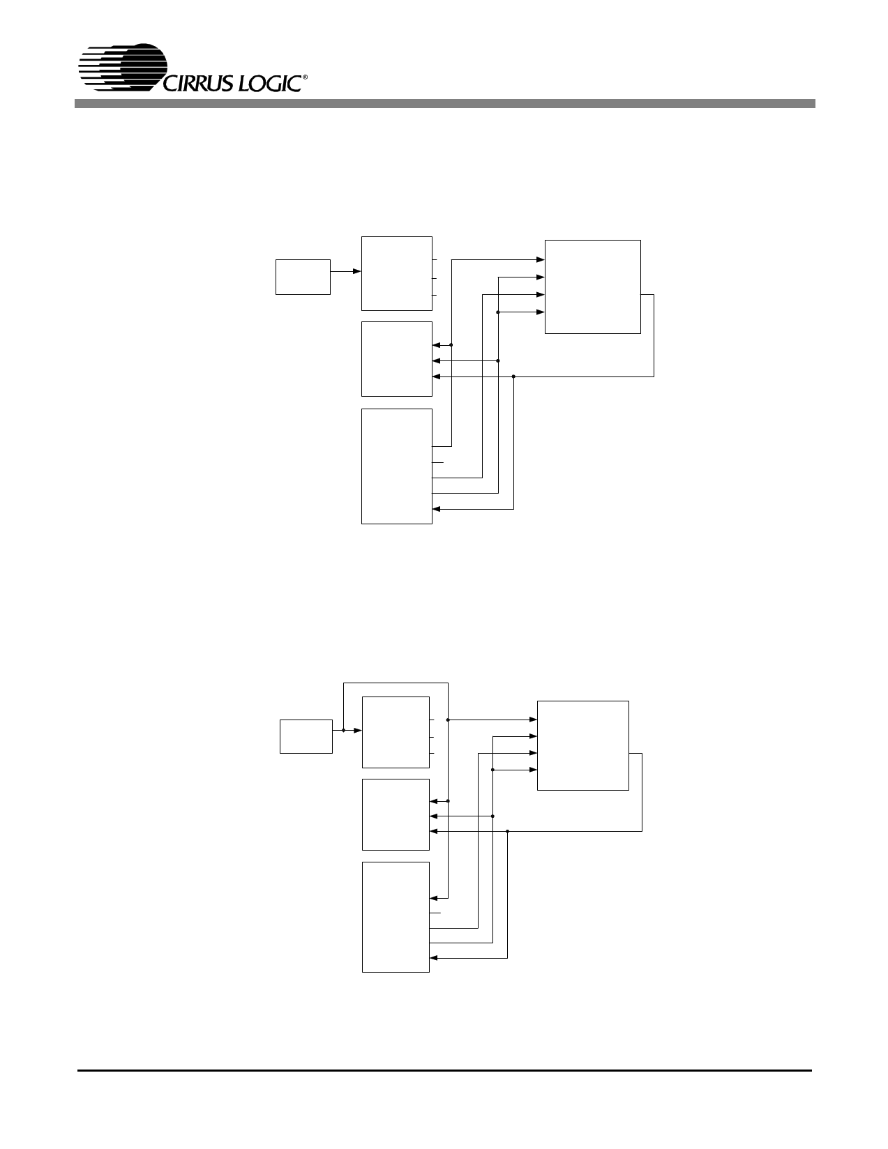
1.7.3a Setup 7
An external DSP connected to DSP I/O HDR masters all clocks for the ADC/DAC and pro-
vides data to the DAC. Subclocks for the ADC/DAC are input via DSP_ADC_LRCK and
DSP_ADC_SCLK. For implementation of this setup option, set DIP switch S4 (SW[3:0])
to ‘0111’b.
AUDIO
MCLK
CS8416
OMCK
RM CK
OL RC K /
OSCLK
S DO U T
CS8406
OM CK
IL RC K /
IS C LK
SD IN
CS42406
M C LK
DAC_LRCK/
DAC_SCLK
D A C _S D INx
ADC_L RCK/
AD C _S C LK
A D C_ S DO U T
DSP I/O
HDR
DSP_ MCLK
DSP_ DAC_L RCK/
DSP_ DAC_SCLK
D S P _S D IN x
DSP_ ADC_L RCK/
DSP_ ADC_SCLK
D S P _S DO U T
Figure 8. DSP Routing - Setup 7
1.7.3b Setup 8
Using the on-board crystal oscillator, AUDIO MCLK, a DSP connected to DSP I/O HDR
masters the subclocks for the ADC/DAC and provides data to the DAC. Subclocks for the
ADC/DAC are input via DSP_ADC_LRCK and DSP_ADC_SCLK. For implementation of
this setup option, set DIP switch S4 (SW[3:0]) to ‘1000’b.
AUDIO
MCLK
CS8416
RMCK
OMCK
OLRC K/
OSC LK
SD OUT
CS 8406
OMCK
ILRCK /
ISCLK
SD IN
CS42406
MCLK
DAC _LRCK/
DAC _SCLK
DAC _SDINx
AD C_LRCK/
AD C_SC LK
ADC _SDOU T
DSP I/O
HDR
DS P_M CLK
DS P_DA C_LRCK /
DS P_DA C_SCLK
DSP_SDIN x
DSP_AD C_LRCK/
DSP_AD C_SCLK
DSP_SD OUT
Figure 9. DSP Routing - Setup 8
11
11 Page | ||
| Páginas | Total 30 Páginas | |
| PDF Descargar | [ Datasheet CDB42406.PDF ] | |
Hoja de datos destacado
| Número de pieza | Descripción | Fabricantes |
| CDB42406 | Evaluation Board | Cirrus Logic |
| Número de pieza | Descripción | Fabricantes |
| SLA6805M | High Voltage 3 phase Motor Driver IC. |
Sanken |
| SDC1742 | 12- and 14-Bit Hybrid Synchro / Resolver-to-Digital Converters. |
Analog Devices |
|
DataSheet.es es una pagina web que funciona como un repositorio de manuales o hoja de datos de muchos de los productos más populares, |
| DataSheet.es | 2020 | Privacy Policy | Contacto | Buscar |
