|
|
|
PDF ADSP-BF538F Data sheet ( Hoja de datos )
| Número de pieza | ADSP-BF538F | |
| Descripción | Blackfin Embedded Processor | |
| Fabricantes | Analog Devices | |
| Logotipo | ||
Hay una vista previa y un enlace de descarga de ADSP-BF538F (archivo pdf) en la parte inferior de esta página. Total 30 Páginas | ||
|
No Preview Available !
www.DataSheet4U.com
a
Preliminary Technical Data
FEATURES
Up to 500 MHz high performance Blackfin processor
Two 16-bit MACs, two 40-bit ALUs, four 8-bit video ALUs,
40-bit shifter
RISC-like register and instruction model for ease of pro-
gramming and compiler friendly support
Advanced debug, trace, and performance monitoring
0.8 V to 1.2 V core VDD with on-chip voltage regulation
3.3 V tolerant I/O with specific 5 V tolerant pins
316-ball Pb-free mini-BGA package
MEMORY
148K bytes of on-chip memory:
16K bytes of instruction SRAM/cache
64K bytes of instruction SRAM
32K bytes of data SRAM
32K bytes of data SRAM/cache
4K bytes of scratchpad SRAM
512K bytes or 1M byte of flash memory (ADSP-BF538F parts
only)
Four dual-channel memory DMA controllers
Blackfin®
Embedded Processor
ADSP-BF538/ADSP-BF538F
Memory management unit providing memory protection
External memory controller with glueless support
for SDRAM, SRAM, flash, and ROM
Flexible memory booting options from SPI® and external
memory
PERIPHERALS
Parallel peripheral interface (PPI/GPIO)
supporting ITU-R 656 video data formats
Four dual-channel, full-duplex synchronous serial ports, sup-
porting 16 stereo I2S® channels
Two DMA controllers supporting 26 DMA channels
Controller area network (CAN) 2.0B controller
Three SPI-compatible ports
Three timer/counters with PWM support
Three UARTs with support for IrDA®
Two TWI controllers compatible with I2C® industry standard
Up to 54 general-purpose I/O pins (GPIO)
Real time clock, watchdog timer, and core timer
On-chip PLL capable of 0.5x To 64x frequency multiplication
Debug/JTAG interface
VOLTAGE REGULATOR
JTAG TEST AND EMULATION
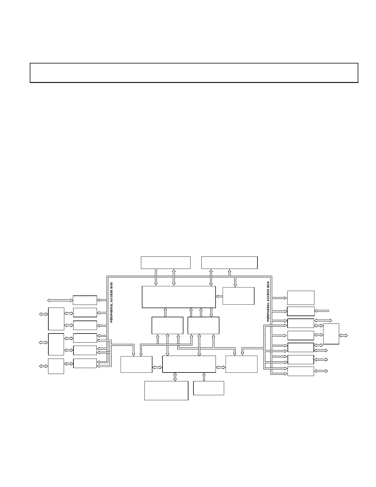
GPIO
PORT
C
GPIO
PORT
D
GPIO
PORT
E
TWI0-1
CAN 2.0B
GPIO
SPI1-2
UART1-2
SPORT2-3
B
INTERRUPT
CONTROLLER
L1
INSTRUCTION
MEMORY
DMA ACCESS DMA CORE
BUS 1
BUS 1
L1
DATA
MEMORY
DMA CORE
BUS 0
DMA ACCESS
BUS 0
DMA
CONTROLLER1
EXTERNAL PORT
FLASH, SDRAM CONTROL
DMA
CONTROLLER0
DMA
E XTERNAL
BUS 1
DMA
EXTERNAL
BUS 0
512 KB OR 1 MB
FLASH MEMORY
(ADSP-BF538F ONLY)
BOOT ROM
WATCHDOG
TIMER
RTC
PPI
TIMER0-2
SPI0
UART0
SPORT0-1
GPIO
PORT
F
Figure 1. Functional Block Diagram
Blackfin and the Blackfin logo are registered trademarks of Analog Devices, Inc.
Rev. PrD
Information furnished by Analog Devices is believed to be accurate and reliable.
However, no responsibility is assumed by Analog Devices for its use, nor for any
infringements of patents or other rights of third parties that may result from its use.
Specifications subject to change without notice. No license is granted by implication
or otherwise under any patent or patent rights of Analog Devices. Trademarks and
registered trademarks are the property of their respective owners.
One Technology Way, P.O. Box 9106, Norwood, MA 02062-9106 U.S.A.
Tel: 781.329.4700
www.analog.com
Fax: 781.461.3113 © 2006 Analog Devices, Inc. All rights reserved.
1 page 
Preliminary Technical Data
Blackfin processors support a modified Harvard architecture in
combination with a hierarchical memory structure. Level 1 (L1)
memories are those that typically operate at the full processor
speed with little or no latency. At the L1 level, the instruction
memory holds instructions only. The two data memories hold
data, and a dedicated scratchpad data memory stores stack and
local variable information.
In addition, multiple L1 memory blocks are provided, offering a
configurable mix of SRAM and cache. The Memory Manage-
ment Unit (MMU) provides memory protection for individual
tasks that may be operating on the core and can protect system
registers from unintended access.
The architecture provides three modes of operation: User mode,
Supervisor mode, and Emulation mode. User mode has
restricted access to certain system resources, thus providing a
protected software environment, while supervisor mode has
unrestricted access to the system and core resources.
The Blackfin processor instruction set has been optimized so
that 16-bit opcodes represent the most frequently used instruc-
tions, resulting in excellent compiled code density. Complex
DSP instructions are encoded into 32-bit opcodes, representing
fully featured multifunction instructions. Blackfin processors
support a limited multi-issue capability, where a 32-bit instruc-
tion can be issued in parallel with two 16-bit instructions,
allowing the programmer to use many of the core resources in a
single instruction cycle.
The Blackfin processor assembly language uses an algebraic syn-
tax for ease of coding and readability. The architecture has been
optimized for use in conjunction with the C/C++ compiler,
resulting in fast and efficient software implementations.
MEMORY ARCHITECTURE
The ADSP-BF538/ADSP-BF538F processors view memory as a
single unified 4 Gbyte address space, using 32-bit addresses. All
resources, including internal memory, external memory, and
I/O control registers, occupy separate sections of this common
address space. The memory portions of this address space are
arranged in a hierarchical structure to provide a good cost/per-
formance balance of some very fast, low latency on-chip
memory as cache or SRAM, and larger, lower cost and perfor-
mance off-chip memory systems. See Figure 3.
The L1 memory system is the primary highest performance
memory available to the Blackfin processor. The off-chip mem-
ory system, accessed through the External Bus Interface Unit
(EBIU), provides expansion with SDRAM, flash memory, and
SRAM, optionally accessing up to 132 Mbytes of physical
memory.
The memory DMA controllers provide high bandwidth data
movement capability. They can perform block transfers of code
or data between the internal memory and the external memory
spaces.
ADSP-BF538/ADSP-BF538F
0xFFFF FFFF
0xFFE0 0000
0xFFC0 0000
0xFFB0 1000
0xFFB0 0000
0xFFA1 4000
0xFFA1 0000
0xFFA0 8000
0xFF90 8000
0xFF90 4000
0xFF80 8000
0xFF80 4000
0xEF00 0000
0x2040 0000
0x2030 0000
0x2020 0000
0x2010 0000
0x2000 0000
0x0800 0000
0x0000 0000
CORE MMR REGISTERS (2M BYTE)
SYSTEM MMR REGISTERS (2M BYTE)
RESERVED
SCRATCHPAD SRAM (4K BYTE)
RESERVED
INSTRUCTION SRAM / CACHE (16K BYTE)
INSTRUCTION SRAM (32K BYTE)
RESERVED
DATA BANK B SRAM / CACHE (16K BYTE)
RESERVED
DATA BANK A SRAM / CACHE (16K BYTE)
RESERVED
RESERVED
ASYNC MEMORY BANK 3 (1M BYTE) OR
ON-CHIP FLASH
ASYNC MEMORY BANK 2 (1M BYTE) OR
ON-CHIP FLASH
ASYNC MEMORY BANK 1 (1M BYTE) OR
ON-CHIP FLASH
ASYNC MEMORY BANK 0 (1M BYTE) OR
ON-CHIP FLASH
RESERVED
SDRAM MEMORY (16M BYTE - 128M BYTE)
Figure 3. ADSP-BF538/ADSP-BF538F Internal/External Memory Map
Internal (On-chip) Memory
The ADSP-BF538/ADSP-BF538F processors have three blocks
of on-chip memory providing high bandwidth access to the
core.
The first is the L1 instruction memory, consisting of 80 Kbytes
SRAM, of which 16 Kbytes can be configured as a four way set-
associative cache. This memory is accessed at full processor
speed.
The second on-chip memory block is the L1 data memory, con-
sisting of two banks of up to 32 Kbytes each. Each memory bank
is configurable, offering both two-way set-associative cache and
SRAM functionality. This memory block is accessed at full pro-
cessor speed.
The third memory block is a 4K byte scratchpad SRAM which
runs at the same speed as the L1 memories, but is only accessible
as data SRAM and cannot be configured as cache memory.
External (Off-Chip) Memory
External memory is accessed via the EBIU. This 16-bit interface
provides a glueless connection to a bank of synchronous DRAM
(SDRAM) as well as up to four banks of asynchronous memory
devices including flash, EPROM, ROM, SRAM, and memory
mapped I/O devices.
Rev. PrD | Page 5 of 56 | May 2006
5 Page 
Preliminary Technical Data
DMA channels, one for transmit and one for receive. These
DMA channels have lower default priority than most DMA
channels because of their relatively low service rates.
The UART port's baud rate, serial data format, error code gen-
eration and status, and interrupts are programmable:
• Supporting bit rates ranging from (fSCLK/ 1,048,576) to
(fSCLK/16) bits per second.
• Supporting data formats from 7 to12 bits per frame.
• Both transmit and receive operations can be configured to
generate maskable interrupts to the processor.
The UART port’s clock rate is calculated as:
UART Clock Rate
=
------------------f-S---C---L---K-------------------
16 × UART_Divisor
Where the 16-bit UART_Divisor comes from the UARTx_DLH
register (most significant 8 bits) and UARTx_DLL register (least
significant 8 bits).
In conjunction with the general-purpose timer functions, auto-
baud detection is supported.
The capabilities of the UARTs are further extended with sup-
port for the Infrared Data Association (IrDA®) Serial Infrared
Physical Layer Link Specification (SIR) protocol.
GENERAL-PURPOSE PORTS
The ADSP-BF538/ADSP-BF538F processors have up to 54 gen-
eral-purpose I/O pins that are multiplexed with other
peripherals. They are arranged into ports C, D, E, and F as
shown in Table 4.
The general-purpose I/O pins may be individually controlled by
manipulation of the control and status registers. These pins may
be polled to determine their status.
• GPIO direction control register – Specifies the direction of
each individual GPIOx pin as input or output.
• GPIO control and status registers – The processor employs
a “write one to modify” mechanism that allows any combi-
nation of individual GPIO to be modified in a single
instruction, without affecting the level of any other GPIO.
Four control registers and a data register are provided for
each GPIO port. One register is written in order to set
GPIO values, one register is written in order to clear GPIO
values, one register is written in order to toggle GPIO val-
ues, and one register is written in order to specify a GPIO
input or output. Reading the GPIO Data allows software to
determine the state of the input GPIO pins.
In addition to the GPIO function described above, the 16 port F
pins can be individually configured to generate interrupts.
• Flag interrupt mask registers – The two Flag interrupt
mask registers allow each individual PFx pin to function as
an interrupt to the processor. similar to the two flag control
registers that are used to set and clear individual flag values,
one flag interrupt mask register sets bits to enable interrupt
function, and the other flag interrupt mask register clears
bits to disable interrupt function. PFx pins defined as
ADSP-BF538/ADSP-BF538F
inputs can be configured to generate hardware interrupts,
while output PFx pins can be triggered by software
interrupts.
• Flag interrupt sensitivity registers – The two flag interrupt
sensitivity registers specify whether individual PFx pins are
level- or edge-sensitive and specify—if edge-sensitive—
whether just the rising edge or both the rising and falling
edges of the signal are significant. One register selects the
type of sensitivity, and one register selects which edges are
significant for edge-sensitivity.
Table 4. GPIO Ports
Peripheral
PPI
SPORT2
SPORT3
SPI1
SPI2
UART1
UART2
CAN
GPIO
Alternate GPIO Port Function
GPIO Port F15–0
GPIO Port E7–0
GPIO Port E15–8
GPIO Port D4–0
GPIO Port D9–5
GPIO Port D11–10
GPIO Port D13–12
GPIO Port C1–0
GPIO Port C9–4
PARALLEL PERIPHERAL INTERFACE
The ADSP-BF538/ADSP-BF538F processors provide a parallel
peripheral interface (PPI) that can connect directly to parallel
A/D and D/A converters, video encoders and decoders, and
other general-purpose peripherals. The PPI consists of a dedi-
cated input clock pin, up to 3 frame synchronization pins, and
at up to 16 data pins. The input clock supports parallel data rates
at up to fSCLK/2 MHz, and the synchronization signals can be con-
figured as either inputs or outputs.
The PPI supports a variety of general-purpose and ITU-R 656
modes of operation. In general-purpose mode, the PPI provides
half-duplex, bi-directional data transfer with up to 16 bits of
data. Up to 3 frame synchronization signals are also provided.
In ITU-R 656 mode, the PPI provides half-duplex, bi-direc-
tional transfer of 8- or 10-bit video data. Additionally, on-chip
decode of embedded start-of-line (SOL) and start-of-field (SOF)
preamble packets is supported.
General-Purpose Mode Descriptions
The general-purpose modes of the PPI are intended to suit a
wide variety of data capture and transmission applications.
Three distinct submodes are supported:
• Input mode – frame syncs and data are inputs into the PPI.
• Frame capture mode – frame syncs are outputs from the
PPI, but data are inputs.
• Output mode – frame syncs and data are outputs from the
PPI.
Rev. PrD | Page 11 of 56 | May 2006
11 Page | ||
| Páginas | Total 30 Páginas | |
| PDF Descargar | [ Datasheet ADSP-BF538F.PDF ] | |
Hoja de datos destacado
| Número de pieza | Descripción | Fabricantes |
| ADSP-BF538 | Blackfin Embedded Processor | Analog Devices |
| ADSP-BF538F | Blackfin Embedded Processor | Analog Devices |
| Número de pieza | Descripción | Fabricantes |
| SLA6805M | High Voltage 3 phase Motor Driver IC. |
Sanken |
| SDC1742 | 12- and 14-Bit Hybrid Synchro / Resolver-to-Digital Converters. |
Analog Devices |
|
DataSheet.es es una pagina web que funciona como un repositorio de manuales o hoja de datos de muchos de los productos más populares, |
| DataSheet.es | 2020 | Privacy Policy | Contacto | Buscar |