|
|
|
PDF ADSP-BF534 Data sheet ( Hoja de datos )
| Número de pieza | ADSP-BF534 | |
| Descripción | (ADSP-BF534 - ADSP-BF537) Blackfin Embedded Processor | |
| Fabricantes | Analog Devices | |
| Logotipo | ||
Hay una vista previa y un enlace de descarga de ADSP-BF534 (archivo pdf) en la parte inferior de esta página. Total 30 Páginas | ||
|
No Preview Available !
www.DataSheet4U.com
a
Blackfin®
Embedded Processor
ADSP-BF534/ADSP-BF536/ADSP-BF537
FEATURES
Up to 600 MHz high performance Blackfin processor
Two 16-bit MACs, two 40-bit ALUs, four 8-bit video ALUs,
40-bit shifter
RISC-like register and instruction model for ease of
programming and compiler-friendly support
Advanced debug, trace, and performance monitoring
0.8 V to 1.2 V core VDD with on-chip voltage regulation
2.5 V and 3.3 V-tolerant I/O with specific 5 V-tolerant pins
182-ball and 208-ball MBGA packages
MEMORY
Up to 132K bytes of on-chip memory comprised of:
Instruction SRAM/cache; instruction SRAM;
data SRAM/cache; additional dedicated data SRAM;
scratchpad SRAM (see Table 1 on Page 3 for available
memory configurations)
External memory controller with glueless support for SDRAM
and asynchronous 8-bit and 16-bit memories
Flexible booting options from external flash, SPI and TWI
memory or from SPI, TWI, and UART host devices
Memory management unit providing memory protection
PERIPHERALS
IEEE 802.3-compliant 10/100 Ethernet MAC (ADSP-BF536 and
ADSP-BF537 only)
Controller area network (CAN) 2.0B interface
Parallel peripheral interface (PPI), supporting ITU-R 656
video data formats
Two dual-channel, full-duplex synchronous serial ports
(SPORTs), supporting eight stereo I2S channels
12 peripheral DMAs, 2 mastered by the Ethernet MAC
Two memory-to-memory DMAs with external request lines
Event handler with 32 interrupt inputs
Serial peripheral interface (SPI)-compatible
Two UARTs with IrDA® support
Two-wire interface (TWI) controller
Eight 32-bit timer/counters with PWM support
Real-time clock (RTC) and watchdog timer
32-bit core timer
48 general-purpose I/Os (GPIOs), 8 with high current drivers
On-chip PLL capable of 1؋ to 63؋ frequency multiplication
Debug/JTAG interface
VOLTAGE REGULATOR
JTAG TEST AND EMULATION
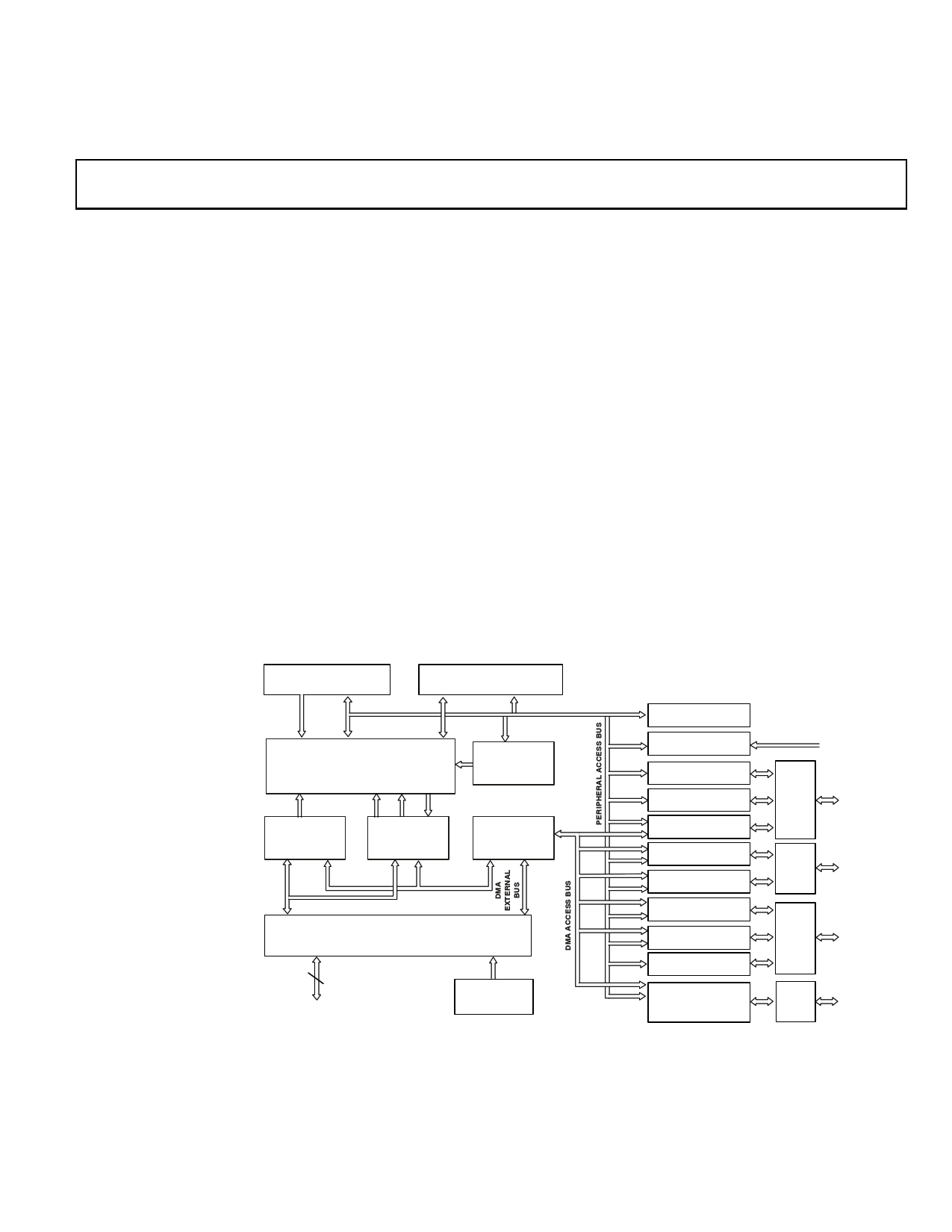
PERIPHERAL ACCESS BUS
WATCHDOG TIMER
B
INTERRUPT
CONTROLLER
RTC
CAN
TWI
L1
INSTRUCTION
MEMORY
EXTERNAL
ACCESS
BUS
L1
DATA
MEMORY
DMA
CONTROLLER
DMA CORE BUS
EXTERNAL PORT
FLASH, SDRAM CONTROL
16
BOOT ROM
SPORT0
SPORT1
PPI
UART 0-1
SPI
TIMERS 0-7
ETHERNET MAC
(ADSP-BF536/
BF537 ONLY)
PORT
J
GPIO
PORT
G
GPIO
PORT
F
GPIO
PORT
H
Figure 1. Functional Block Diagram
Blackfin and the Blackfin logo are registered trademarks of Analog Devices, Inc.
Rev. B
Information furnished by Analog Devices is believed to be accurate and reliable.
However, no responsibility is assumed by Analog Devices for its use, nor for any
infringements of patents or other rights of third parties that may result from its use.
Specifications subject to change without notice. No license is granted by implication
or otherwise under any patent or patent rights of Analog Devices. Trademarks and
registered trademarks are the property of their respective owners.
One Technology Way, P.O. Box 9106, Norwood, MA 02062-9106 U.S.A.
Tel: 781.329.4700
Fax: 781.461.3113
www.analog.com
©2006 Analog Devices, Inc. All rights reserved.
1 page 
The address arithmetic unit provides two addresses for simulta-
neous dual fetches from memory. It contains a multiported
register file consisting of four sets of 32-bit index, modify,
length, and base registers (for circular buffering), and eight
additional 32-bit pointer registers (for C-style indexed stack
manipulation).
Blackfin processors support a modified Harvard architecture in
combination with a hierarchical memory structure. Level 1 (L1)
memories are those that typically operate at the full processor
speed with little or no latency. At the L1 level, the instruction
memory holds instructions only. The two data memories hold
data, and a dedicated scratchpad data memory stores stack and
local variable information.
In addition, multiple L1 memory blocks are provided, offering a
configurable mix of SRAM and cache. The memory manage-
ment unit (MMU) provides memory protection for individual
tasks that may be operating on the core and can protect system
registers from unintended access.
The architecture provides three modes of operation: user mode,
supervisor mode, and emulation mode. User mode has
restricted access to certain system resources, thus providing a
protected software environment, while supervisor mode has
unrestricted access to the system and core resources.
The Blackfin processor instruction set has been optimized so
that 16-bit opcodes represent the most frequently used instruc-
tions, resulting in excellent compiled code density. Complex
DSP instructions are encoded into 32-bit opcodes, representing
fully featured multifunction instructions. Blackfin processors
support a limited multi-issue capability, where a 32-bit instruc-
tion can be issued in parallel with two 16-bit instructions,
allowing the programmer to use many of the core resources in a
single instruction cycle.
The Blackfin processor assembly language uses an algebraic syn-
tax for ease of coding and readability. The architecture has been
optimized for use in conjunction with the C/C++ compiler,
resulting in fast and efficient software implementations.
MEMORY ARCHITECTURE
The ADSP-BF534/ADSP-BF536/ADSP-BF537 processors view
memory as a single unified 4G byte address space, using 32-bit
addresses. All resources, including internal memory, external
memory, and I/O control registers, occupy separate sections of
this common address space. The memory portions of this
address space are arranged in a hierarchical structure to provide
a good cost/performance balance of some very fast, low latency
on-chip memory as cache or SRAM, and larger, lower cost, and
performance off-chip memory systems. See Figure 3.
The on-chip L1 memory system is the highest performance
memory available to the Blackfin processor. The off-chip mem-
ory system, accessed through the external bus interface unit
(EBIU), provides expansion with SDRAM, flash memory, and
SRAM, optionally accessing up to 516M bytes of
physical memory.
ADSP-BF534/ADSP-BF536/ADSP-BF537
The memory DMA controller provides high bandwidth data-
movement capability. It can perform block transfers of code or
data between the internal memory and the external
memory spaces.
Internal (On-Chip) Memory
The ADSP-BF534/ADSP-BF536/ADSP-BF537 processors have
three blocks of on-chip memory providing high-bandwidth
access to the core.
The first block is the L1 instruction memory, consisting of
64K bytes SRAM, of which 16K bytes can be configured as a
four-way set-associative cache. This memory is accessed at full
processor speed.
The second on-chip memory block is the L1 data memory, con-
sisting of up to two banks of up to 32K bytes each. Each memory
bank is configurable, offering both cache and SRAM functional-
ity. This memory block is accessed at full processor speed.
The third memory block is a 4K byte scratchpad SRAM, which
runs at the same speed as the L1 memories, but is only accessible
as data SRAM, and cannot be configured as cache memory.
External (Off-Chip) Memory
External memory is accessed via the EBIU. This 16-bit interface
provides a glueless connection to a bank of synchronous DRAM
(SDRAM) as well as up to four banks of asynchronous memory
devices including flash, EPROM, ROM, SRAM, and memory
mapped I/O devices.
The PC133-compliant SDRAM controller can be programmed
to interface to up to 512M bytes of SDRAM. A separate row can
be open for each SDRAM internal bank, and the SDRAM con-
troller supports up to 4 internal SDRAM banks, improving
overall performance.
The asynchronous memory controller can be programmed to
control up to four banks of devices with very flexible timing
parameters for a wide variety of devices. Each bank occupies a
1M byte segment regardless of the size of the devices used, so
that these banks are only contiguous if each is fully populated
with 1M byte of memory.
I/O Memory Space
The ADSP-BF534/ADSP-BF536/ADSP-BF537 processors do
not define a separate I/O space. All resources are mapped
through the flat 32-bit address space. On-chip I/O devices have
their control registers mapped into memory-mapped registers
(MMRs) at addresses near the top of the 4G byte address space.
These are separated into two smaller blocks, one which contains
the control MMRs for all core functions, and the other which
contains the registers needed for setup and control of the on-
chip peripherals outside of the core. The MMRs are accessible
only in supervisor mode and appear as reserved space to on-
chip peripherals.
Rev. B | Page 5 of 68 | July 2006
5 Page 
ADSP-BF534/ADSP-BF536/ADSP-BF537
In conjunction with the general-purpose timer functions, auto-
baud detection is supported.
The capabilities of the UARTs are further extended with sup-
port for the infrared data association (IrDA) serial infrared
physical layer link specification (SIR) protocol.
CONTROLLER AREA NETWORK (CAN)
The ADSP-BF534/ADSP-BF536/ADSP-BF537 processors offer
a CAN controller that is a communication controller imple-
menting the CAN 2.0B (active) protocol. This protocol is an
asynchronous communications protocol used in both industrial
and automotive control systems. The CAN protocol is well-
suited for control applications due to its capability to communi-
cate reliably over a network, since the protocol incorporates
CRC checking message error tracking, and fault node
confinement.
The CAN controller offers the following features:
• 32 mailboxes (eight receive only, eight transmit only, 16
configurable for receive or transmit).
• Dedicated acceptance masks for each mailbox.
• Additional data filtering on first two bytes.
• Support for both the standard (11-bit) and extended
(29-bit) identifier (ID) message formats.
• Support for remote frames.
• Active or passive network support.
• CAN wakeup from hibernation mode (lowest static power
consumption mode).
• Interrupts, including: Tx complete, Rx complete, error,
global.
The electrical characteristics of each network connection are
very demanding so the CAN interface is typically divided into
two parts: a controller and a transceiver. This allows a single
controller to support different drivers and CAN networks. The
CAN module represents only the controller part of the interface.
The controller interface supports connection to 3.3 V high-
speed, fault-tolerant, single-wire transceivers.
TWI CONTROLLER INTERFACE
The ADSP-BF534/ADSP-BF536/ADSP-BF537 processors
include a 2-wire interface (TWI) module for providing a simple
exchange method of control data between multiple devices. The
TWI is compatible with the widely used I2C® bus standard. The
TWI module offers the capabilities of simultaneous master and
slave operation, support for both 7-bit addressing and multime-
dia data arbitration. The TWI interface utilizes two pins for
transferring clock (SCL) and data (SDA) and supports the
protocol at speeds up to 400k bits/sec. The TWI interface pins
are compatible with 5 V logic levels.
Additionally, the processor’s TWI module is fully compatible
with serial camera control bus (SCCB) functionality for easier
control of various CMOS camera sensor devices.
10/100 ETHERNET MAC
The ADSP-BF536 and ADSP-BF537 processors offer the capa-
bility to directly connect to a network by way of an embedded
Fast Ethernet Media Access Controller (MAC) that supports
both 10-BaseT (10M bits/sec) and 100-BaseT (100M bits/sec)
operation. The 10/100 Ethernet MAC peripheral is fully compli-
ant to the IEEE 802.3-2002 standard, and it provides
programmable features designed to minimize supervision, bus
use, or message processing by the rest of the processor system.
Some standard features are:
• Support of MII and RMII protocols for external PHYs.
• Full duplex and half duplex modes.
• Data framing and encapsulation: generation and detection
of preamble, length padding, and FCS.
• Media access management (in half-duplex operation): col-
lision and contention handling, including control of
retransmission of collision frames and of back-off timing.
• Flow control (in full-duplex operation): generation and
detection of PAUSE frames.
• Station management: generation of MDC/MDIO frames
for read-write access to PHY registers.
• SCLK operating range down to 25 MHz (active and sleep
operating modes).
• Internal loopback from Tx to Rx.
Some advanced features are:
• Buffered crystal output to external PHY for support of a
single crystal system.
• Automatic checksum computation of IP header and IP
payload fields of Rx frames.
• Independent 32-bit descriptor-driven Rx and Tx DMA
channels.
• Frame status delivery to memory via DMA, including
frame completion semaphores, for efficient buffer queue
management in software.
• Tx DMA support for separate descriptors for MAC header
and payload to eliminate buffer copy operations.
• Convenient frame alignment modes support even 32-bit
alignment of encapsulated Rx or Tx IP packet data in mem-
ory after the 14-byte MAC header.
• Programmable Ethernet event interrupt supports any com-
bination of:
• Any selected Rx or Tx frame status conditions.
• PHY interrupt condition.
• Wakeup frame detected.
• Any selected MAC management counter(s) at
half-full.
• DMA descriptor error.
• 47 MAC management statistics counters with selectable
clear-on-read behavior and programmable interrupts on
half maximum value.
Rev. B | Page 11 of 68 | July 2006
11 Page | ||
| Páginas | Total 30 Páginas | |
| PDF Descargar | [ Datasheet ADSP-BF534.PDF ] | |
Hoja de datos destacado
| Número de pieza | Descripción | Fabricantes |
| ADSP-BF531 | Blackfin Embedded Processor | Analog Devices |
| ADSP-BF531SBBC400 | Blackfin Embedded Processor | Analog Devices |
| ADSP-BF531SBBZ400 | Blackfin Embedded Processor | Analog Devices |
| ADSP-BF531SBST400 | Blackfin Embedded Processor | Analog Devices |
| Número de pieza | Descripción | Fabricantes |
| SLA6805M | High Voltage 3 phase Motor Driver IC. |
Sanken |
| SDC1742 | 12- and 14-Bit Hybrid Synchro / Resolver-to-Digital Converters. |
Analog Devices |
|
DataSheet.es es una pagina web que funciona como un repositorio de manuales o hoja de datos de muchos de los productos más populares, |
| DataSheet.es | 2020 | Privacy Policy | Contacto | Buscar |