|
|
|
PDF ADN2880 Data sheet ( Hoja de datos )
| Número de pieza | ADN2880 | |
| Descripción | Transimpedance Amplifier | |
| Fabricantes | Analog Devices | |
| Logotipo | ||
Hay una vista previa y un enlace de descarga de ADN2880 (archivo pdf) en la parte inferior de esta página. Total 12 Páginas | ||
|
No Preview Available !
www.DataSheet4U.com
FEATURES
Bandwidth: 2.5 GHz
Optical sensitivity: −24.2 dBm1
Differential transimpedance: 4400 V/A
Power dissipation: 70 mW
Differential output swing: 260 mV p-p
Input overload current: 4.3 mA p-p
On-chip RSSI function
Low frequency cutoff: 20 kHz
On-chip PD filter: RF = 200 Ω, CF = 20 pF
Die size: 0.7 mm × 1.2 mm
APPLICATIONS
3.2 Gbps or below optical receivers
SONET/GbE/FC optical receivers
SFF-8472-compliant receivers
PIN/APD-TIA receive optical subassemblies (ROSA)
3.2 Gbps, 3.3 V, Low Noise,
Transimpedance Amplifier
ADN2880
GENERAL DESCRIPTION
The ADN2880 is a 3.3 V, high gain SiGe transimpedance
amplifier (TIA). The TIA converts the small signal current of a
photo detector into differential voltage output. The ADN2880
features a 315 nA typical input-referred noise, enabling an
optical sensitivity of −24.2 dBm (0.85 A/W PIN). With a
bandwidth of 2.5 GHz, the ADN2880 allows a data rate
operation up to 3.2 Gbps. Typical power dissipation is
approximately 70 mW.
To facilitate the assembly in small form factor packages, such
as TO-46 headers, the ADN2880 provides an on-chip RC filter
(200 Ω, 20 pF) and features a 20 kHz low frequency cutoff
without using an external capacitor. An on-chip RSSI circuit,
which generates a voltage proportional to the average photo-
diode current, is also available for power monitoring and
assembly alignment.
The ADN2880 is available in die form. With a chip area of
1.2 mm × 0.7 mm, the TIA layout is specifically optimized for
TO-Can-based packages.
1 Based on 1550 nm PIN, responsivity = 0.85 A/W, ER = 9 dB, BER < 10−10.
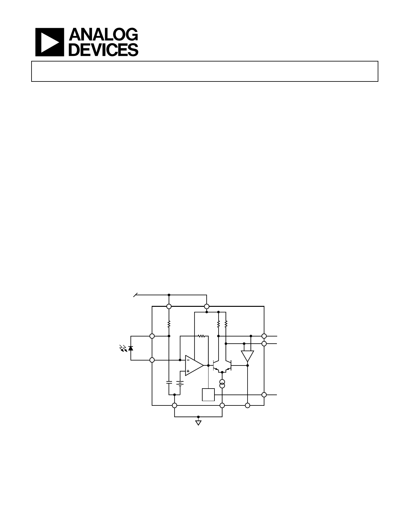
FUNCTIONAL BLOCK DIAGRAM
3.3V
VCCFILTER
VCC
FILTER
IN
200Ω
50Ω
1400Ω
50Ω
OUT
OUTB
20pF
0.85V
GND
5mA
RSSI
GND CAP
Figure 1.
Rev. 0
Information furnished by Analog Devices is believed to be accurate and reliable. However, no
responsibility is assumed by Analog Devices for its use, nor for any infringements of patents or other
rights of third parties that may result from its use. Specifications subject to change without notice. No
license is granted by implication or otherwise under any patent or patent rights of Analog Devices.
Trademarksandregisteredtrademarksarethepropertyoftheirrespectiveowners.
One Technology Way, P.O. Box 9106, Norwood, MA 02062-9106, U.S.A.
Tel: 781.329.4700
www.analog.com
Fax: 781.461.3113
© 2005 Analog Devices, Inc. All rights reserved.
1 page 
PAD LAYOUT AND FUNCTION DESCRIPTIONS
VCC
VCC
VCCFILTER
GND
ADN2880
GND
IN
TEST
FILTER
FILTER
1 17 16 15
2
3
4
5 678
14
9
13 GND
12 OUT
11 OUTB
10 GND
GND
RSSI
CAP
GND
Figure 2. Pad Layout
Table 3. Pad Function Descriptions
Pad No.
Mnemonic Pin Type1
1 GND P
2 IN AI
3
TEST
AI
4, 5
FILTER
AO
6 GND P
7 RSSI AO
8 CAP AI
9, 10, 13, 14
11
12
15
GND
OUTB
OUT
VCCFILTER
P
AO
AO
P
16, 17
VCC
P
Description
Ground. (Input return.)
Current Input. Bond directly to a photodiode (PD) anode.
Test Probe Pad. Do not connect.
Filter Output. Pad 4 and Pad 5 are metal connected. Optional bond to a PD cathode.
Ground.
Voltage Output. Provides average input current monitoring. If not used, connect to ground.
Low Frequency Cutoff (LFC) Setpoint. For SONET applications, see Figure 10 and contact sales
for assembly details.
Ground. (Output return.)
Negative Output, CML, On-Chip 50 Ω Termination (AC or DC Termination).
Positive Output, CML, On-Chip 50 Ω Termination (AC or DC Termination).
On-Chip Filter Supply. Connect to VCC to Enable On-Chip RC Filter (200 Ω, 20 pF). Leave
unconnected if not used.
3.3 V Supply. Place a 200 pF, RF decoupling capacitor close to the power pad to reduce
the power noise.
1 P = power; AI = analog input; and AO = analog output.
Rev. 0 | Page 5 of 12
5 Page 
PIN Photodiode for Non-SDH/SONET Applications
VCC
OUTB
CB
SC OUT
ADN2880
OUTB
VCC
SC
CB
OUT
Figure 26. Coplanar PIN for a 4-Pin TO-46
VCC B.W.
CB
B.W.
B.W.
VCCFILTER
VCC
B.W.
FILTER
B.W. IN
200Ω
50Ω 50Ω
B.W.
B.W.
OUT
OUTB
20pF
0.85V
RSSI
GND
B.W.
GND
B.W.
CAP
Figure 27. Equivalent Circuit with Bond Wires, as Shown in Figure 26
Table 6. Bill of Materials (BOM)
Component Description
PD 1× vendor specific, 2.5 Gbps, photodiode
TIA 1× ADN2880 (0.7 mm × 1.2 mm), 3.2 Gbps,
transimpedance amplifier
CB 1× 200 pF, RF single-layer capacitor
Sc 1× ceramic standoff or 1× optional 1000 pF
capacitor
Figure 28. Dual Planar PIN for a 4-Pin TO-46
ADN2880 PD
SC
CB
TO CAN HEADER
Figure 29. Side View of the Assembly, as Shown in Figure 26
Notes
One mil thickness, gold wire, ball bond recommended.
Minimize all GND bond-wire lengths.
Minimize IN, FILTER, OUT, and OUTB bond-wire lengths.
Maintain symmetry in length and orientation between OUT
and OUTB bond wires.
Maintain symmetry in length and orientation between IN and
FILTER bond wires.
Maintain symmetry between IN/FILTER and OUT/OUTB
bond wires.
Rev. 0 | Page 11 of 12
11 Page | ||
| Páginas | Total 12 Páginas | |
| PDF Descargar | [ Datasheet ADN2880.PDF ] | |
Hoja de datos destacado
| Número de pieza | Descripción | Fabricantes |
| ADN2880 | Transimpedance Amplifier | Analog Devices |
| ADN2882 | Low Noise Transimpedance Amplifier | Analog Devices |
| Número de pieza | Descripción | Fabricantes |
| SLA6805M | High Voltage 3 phase Motor Driver IC. |
Sanken |
| SDC1742 | 12- and 14-Bit Hybrid Synchro / Resolver-to-Digital Converters. |
Analog Devices |
|
DataSheet.es es una pagina web que funciona como un repositorio de manuales o hoja de datos de muchos de los productos más populares, |
| DataSheet.es | 2020 | Privacy Policy | Contacto | Buscar |