|
|
|
PDF ADN2818 Data sheet ( Hoja de datos )
| Número de pieza | ADN2818 | |
| Descripción | (ADN2817 / ADN2818) Clock and Data Recovery IC | |
| Fabricantes | Analog Devices | |
| Logotipo | ||
Hay una vista previa y un enlace de descarga de ADN2818 (archivo pdf) en la parte inferior de esta página. Total 30 Páginas | ||
|
No Preview Available !
www.DataSheet4U.com
Preliminary Technical Data
Continuous Rate 12.3Mb/s to 2.7Gb/s
Clock and Data Recovery ICs
ADN2817/ADN2818
FEATURES
Serial data input: 12.3 Mb/s to 2.7 Gb/s
Exceeds ITU-T Jitter Specifications
Integrated Limiting Amp: 6mV sensitivity (ADN2817 only)
Adjustable slice level: ±100 mV (ADN2817 only)
Patented dual-loop clock recovery architecture
Programmable LOS detect (ADN2817 only)
Slice level and sample phase adjustments (ADN2817 only)
Integrated PRBS Generator and Detector
No reference clock required
Loss of lock indicator
Supports Double Data Rate
Relative Bit Error Rate Monitor
Rate Selectivity without the use of a reference clock
I2C™ interface to access optional features
Single-supply operation: 3.3 V
Low power: 650/600 mW (ADN2817/ADN2818)
5 mm × 5 mm 32-lead LFCSP
APPLICATIONS
SONET OC-1/3/12/48 and all associated FEC rates
Fibre Channel, 2× Fibre Channel , GbE, HDTV, etc.
WDM transponders
Regenerators/repeaters
Test equipment
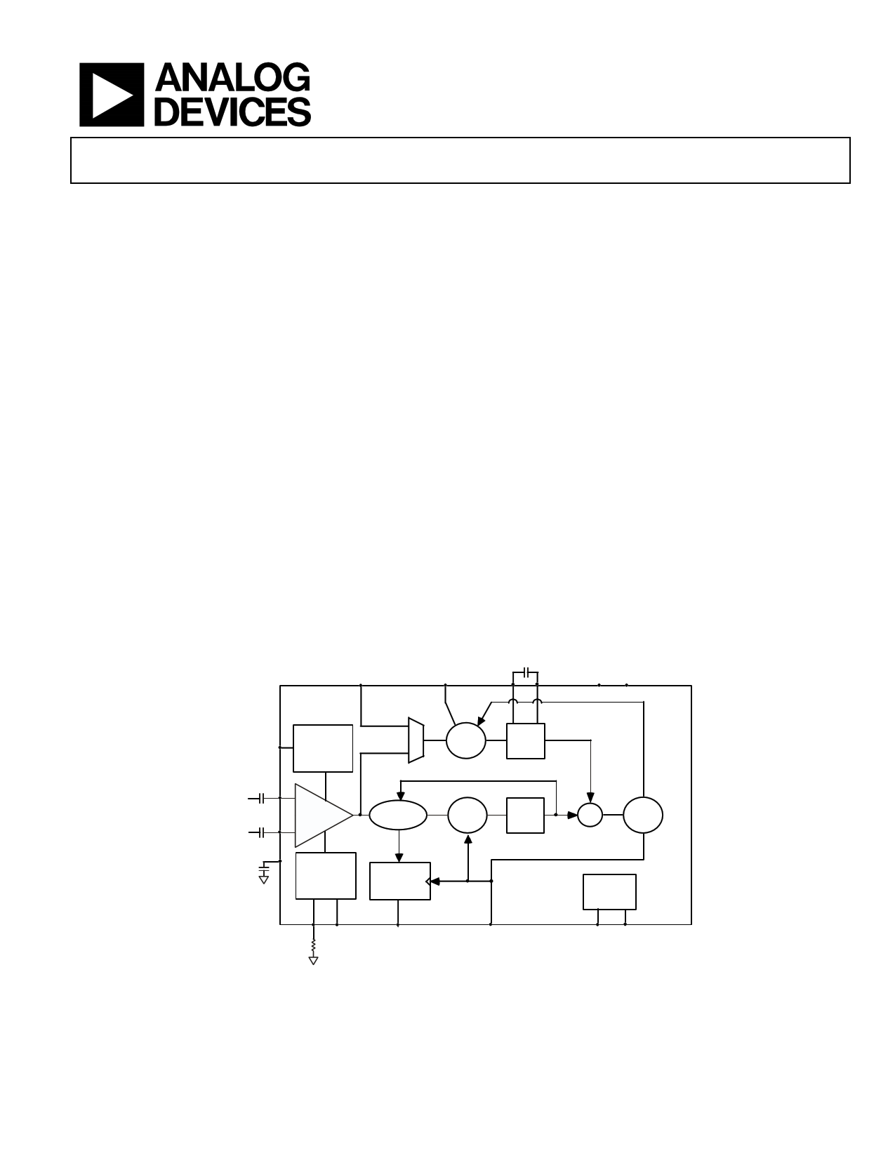
FUNCTIONAL
BLOCK DIAGRAM
REFCLKP/N
(optional)
LOL
PRODUCT DESCRIPTION
The ADN2817/ADN2818 provides the receiver functions of
quantization, signal level detect, and clock and data recovery for
continuous data rates from 12.3 Mb/s to 2.7 Gb/s. The
ADN2817/ADN2818 automatically locks to all data rates
without the need for an external reference clock or
programming. All SONET jitter requirements are exceeded,
including jitter transfer, jitter generation, and jitter tolerance.
All specifications are quoted for −40°C to +85°C ambient
temperature, unless otherwise noted.
This device, together with a PIN diode and a TIA preamplifier,
can implement a highly integrated, low cost, low power fiber
optic receiver.
The ADN2817/ADN2818 have many optional features available
via an I2C interface, e.g. the user can read back the data rate that
the ADN2817/ADN2818 is locked on to, or the user can set the
device to only lock to one particular data rate if provisioning of
data rates is required.
The ADN2817/ADN2818 is available in a compact 5 mm × 5
mm 32-lead chip scale package.
CF1 CF2 VCC VEE
SLICEP/N
Slice Adjust
(ADN2817
only)
PIN
NIN
Phase
Shifter
VREF
LOS Detect
(ADN2817
only)
Data
Re-Timing
Freq/
Lock
Det
Phase
Det.
Loop
Filter
Loop
Filter
THRADJ SDOUT DATAOUTP/N
CLKOUTP/N
Σ VCO
I2C
Registers
SCK SDA
Figure 1 ADN2817/ADN2818 Functional Block Diagram
Rev.PrA
Information furnished by Analog Devices is believed to be accurate and reliable.
However, no responsibility is assumed by Analog Devices for its use, nor for any
infringements of patents or other rights of third parties that may result from its use.
Specifications subject to change without notice. No license is granted by implication
or otherwise under any patent or patent rights of Analog Devices. Trademarks and
registered trademarks are the property of their respective owners.
One Technology Way, P.O. Box 9106, Norwood, MA 02062-9106, U.S.A.
Tel: 781.329.4700
www.analog.com
Fax: 781.326.8703 © 2006 Analog Devices, Inc. All rights reserved.
1 page 
Preliminary Technical Data
ADN2817/ADN2818
OUTPUT AND TIMING SPECIFICATIONS
Table 3.
Parameter
CML OUPUT CHARACTERISTICS
(CLKOUTP/N, DATAOUTP/N)
Single-Ended Output Swing
Differential Output Swing
Output High Voltage
Output Low Voltage
CML Ouputs Timing
Rise Time
Fall Time
Setup Time
Hold Time
I2C INTERFACE DC CHARACTERISTICS
Input High Voltage
Input Low Voltage
Input Current
Output Low Voltage
I2C INTERFACE TIMING
SCK Clock Frequency
SCK Pulse Width High
SCK Pulse Width Low
Start Condition Hold Time
Start Condition Setup Time
Data Setup Time
Data Hold Time
SCK/SDA Rise/Fall Time
Stop Condition Setup Time
Bus Free Time between a Stop and a Start
REFCLK CHARACTERISTICS
Input Voltage Range
Minimum Differential Input Drive
Reference Frequency
Required Accuracy
LVTTL DC INPUT CHARACTERISTICS
Input High Voltage
Input Low Voltage
Input High Current
Input Low Current
LVTTL DC OUTPUT CHARACTERISTICS
Output High Voltage
Output Low Voltage
Conditions
VSE (see Figure 3)
VDIFF (see Figure 3)
VOH
VOL
20% to 80%
80% to 20%
TS (see Figure 2), OC-48
TH (see Figure 2), OC-48
LVCMOS
VIH
VIL
VIN = 0.1 VCC or VIN = 0.9 VCC
VOL, IOL = 3.0 mA
(See Figure 11)
tHIGH
tLOW
tHD;STA
tSU;STA
tSU;DAT
tHD;DAT
TR/TF
tSU;STO
tBUF
Optional lock to REFCLK mode
@ REFCLKP or REFCLKN
VIL
VIH
VIH
VIL
IIH, VIN = 2.4 V
IIL, VIN = 0.4 V
VOH, IOH = −2.0 mA
VOL, IOL = 2.0 mA
Min
300
600
VCC − 0.6
150
150
0.7 VCC
−10.0
600
1300
600
600
100
300
20 + 0.1 Cb1
600
1300
12.3
2.0
−5
2.4
Typ Max Unit
350
700
VCC − 0.35
600
1200
VCC
VCC − 0.3
mV
mV
V
V
TBD ps
TBD ps
200 250 ps
200 250 ps
0.3 VCC
+10.0
0.4
V
V
μA
V
400 kHz
ns
ns
ns
ns
ns
ns
300 ns
ns
ns
0V
VCC V
100 mV p-p
200 MHz
100 ppm
V
0.8 V
5 μA
μA
V
0.4 V
1 Cb = total capacitance of one bus line in pF. If mixed with Hs-mode devices, faster fall-times are allowed (see Table 6).
Rev.Pr A | Page 5 of 35
5 Page 
Preliminary Technical Data
I2C INTERFACE TIMING AND INTERNAL REGISTER DESCRIPTION
SLAVE ADDRESS [6...0]
R/W
CTRL.
1 A5 0 0 0 0 0 X
MSB = 1 SET BY
PIN 19
0 = WR
1 = RD
Figure 7. Slave Address Configuration
ADN2817/ADN2818
S SLAVE ADDR, LSB = 0 (WR) A(S) SUB ADDR A(S) DATA A(S)
Figure 8. I2C Write Data Transfer
DATA A(S) P
S SLAVE ADDR, LSB = 0 (WR) A(S) SUB ADDR A(S) S SLAVE ADDR, LSB = 1 (RD) A(S) DATA A(M)
DATA A(M) P
S = START BIT
A(S) = ACKNOWLEDGE BY SLAVE
P = STOP BIT
A(M) = LACK OF ACKNOWLEDGE BY MASTER
A(M) = ACKNOWLEDGE BY MASTER
Figure 9. I2C Read Data Transfer
START BIT
SDA
SLAVE ADDRESS
A6 A5
SCK
S
SLADDR[4...0]
SUB ADDRESS
A7
A0
DATA
D7
D0
STOP BIT
WR ACK
SUB ADDR[6...1]
Figure 10. I2C Data Transfer Timing
ACK
DATA[6...1]
ACK
P
tF
SDA
SCK
S
tSU;DAT
tHD;STA
tLOW
tR
tF
tSU;STO
tHD;STA
tHD;DAT
tHIGH tSU;STA
S
Figure 11. I2C Port Timing Diagram
tBUF
tR
PS
Rev.Pr A | Page 11 of 35
11 Page | ||
| Páginas | Total 30 Páginas | |
| PDF Descargar | [ Datasheet ADN2818.PDF ] | |
Hoja de datos destacado
| Número de pieza | Descripción | Fabricantes |
| ADN2811 | OC-48/OC-48 FEC Clock and Data Recovery IC | Analog Devices |
| ADN2812 | Continuous Rate 12.3 Mb/s to 2.7 Gb/s Clock and Data Recovery IC with Integrated Limiting Amp | Analog Devices |
| ADN2813 | Clock and Data Recovery IC | Analog Devices |
| ADN2814 | Continuous Rate 12.3 Mb/s to 675 Mb/s Clock and Data Recovery IC | Analog Devices |
| Número de pieza | Descripción | Fabricantes |
| SLA6805M | High Voltage 3 phase Motor Driver IC. |
Sanken |
| SDC1742 | 12- and 14-Bit Hybrid Synchro / Resolver-to-Digital Converters. |
Analog Devices |
|
DataSheet.es es una pagina web que funciona como un repositorio de manuales o hoja de datos de muchos de los productos más populares, |
| DataSheet.es | 2020 | Privacy Policy | Contacto | Buscar |