|
|
|
PDF ADL5519 Data sheet ( Hoja de datos )
| Número de pieza | ADL5519 | |
| Descripción | Dual Log Detector/Controller | |
| Fabricantes | Analog Devices | |
| Logotipo | ||
Hay una vista previa y un enlace de descarga de ADL5519 (archivo pdf) en la parte inferior de esta página. Total 27 Páginas | ||
|
No Preview Available !
www.DataSheet4U.com
Preliminary Technical Data
FEATURES
Wide bandwidth: 1 MHz to 10 GHz
Dual-channel and channel difference outputs ports
Integrated accurately scaled temperature sensor
50 dB dynamic range up to 8 GHz
Stability over temperature ±0.5 dB
Low noise measurement/controller output VOUT
Pulse response time: 8/10 ns (fall/rise)
Small footprint 5 mm x 5 mm LFCSP package
Supply operation: 3.0 V to 5.5 V @ 65 mA
Fabricated using high speed SiGe process
APPLICATIONS
RF transmitter PA setpoint control and level monitoring
Power monitoring in radiolink transmitters
RSSI measurement in base stations, WLAN, WiMAX, radar
Antenna VSWR monitor
Dual-channel wireless infrastructure radios
GENERAL DESCRIPTION
The ADL5519 is a dual-demodulating logarithmic amplifier,
using the AD8317 core. It has the capability of accurately
converting an RF input signal to a corresponding decibel-scaled
output. The ADL5519 provides accurately scaled, independent,
logarithmic outputs of both RF measurement channels.
Difference output ports, which measure the difference between
the two channels, are also available. The on-chip channel
matching makes the log-amp channel difference outputs
extremely stable with temperature and process variations. The
device also includes a useful temperature sensor with an
accurately scaled voltage proportional to temperature, specified
over the device operating temperature range.
The ADL5519 maintains accurate log conformance for signals of
1 MHz to 8 GHz and provides useful operation to 10 GHz. The
input dynamic range is typically 50 dB (re: 50 Ω) with error less
than ±1 dB. The ADL5519 has 8/10 ns response time (fall
time/rise time) that enables RF burst detection to a pulse rate of
beyond 50 MHz. The device provides unprecedented logarithmic
intercept stability vs. ambient temperature conditions. A supply of
3.0 V to 5.5 V is required to power the device. Current
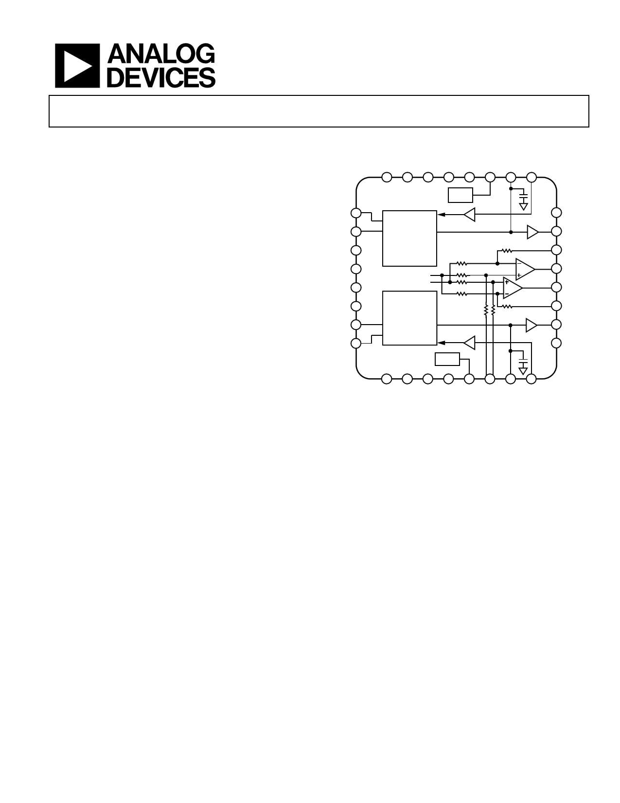
1 MHz to 10 GHz, 50 dB
Dual Log Detector/Controller
ADL5519
INHA 25
INLA 26
COMR 27
PWDN 28
COMR 29
COMR 30
INLB 31
INHB 32
24 23 22 21 20 19 18 17
TEMP
CHANNEL A
Log Detector
OUTA
OUTB
CHANNEL B
Log Detector
BIAS
12345678
25 NC
26 OUTA
27 FBKA
28 OUTP
29 OUTN
30 FBKB
31 OUTB
32 NC
Figure 1. Functional Block Diagram
consumption is typically 65 mA, and it decreases to 1 mA when
the device is disabled.
The device is capable of supplying four log-amp measurements
simultaneously. Linear-in-dB measurements are provided at
OUTA and OUTB, with conveniently scaled slopes of -22
mV/dB. The log-amp difference between OUTA and OUTB is
available as differential or single-ended signals at OUTP and
OUTN. An optional voltage applied to VLVL provides a
common mode reference level to offset OUTP and OUTN
above ground. On-chip wide bandwidth output op amps are
connected to accommodate flexible configurations that support
many system solutions.
The ADL5519 can be easily configured to provide a control
voltage to a power amplifier at any output pin. Since the output
can be used for controller applications, special attention has
been paid to minimize wideband noise
The ADL5519 is fabricated on a SiGe bipolar IC process and is
available in a 5 mm × 5 mm, 32-lead LFCSP package for an
operating temperature range of −40oC to +125oC..
Rev. PrB
Information furnished by Analog Devices is believed to be accurate and reliable. However, no
responsibility is assumed by Analog Devices for its use, nor for any infringements of patents or other
rights of third parties that may result from its use. Specifications subject to change without notice. No
license is granted by implication or otherwise under any patent or patent rights of Analog Devices.
Trademarksandregisteredtrademarksarethepropertyoftheirrespectiveowners.
One Technology Way, P.O. Box 9106, Norwood, MA 02062-9106, U.S.A.
Tel: 781.329.4700
www.analog.com
Fax: 781.461.3113
©2006 Analog Devices, Inc. All rights reserved.
1 page 
Preliminary Technical Data
Parameter
OUT[A, B] Maximum Input Level
OUT[A, B] Minimum Input Level
OUT[A, B, P, N] Slope
OUT[A, B] Intercept
Output Voltage - High Power In
Output Voltage - Low Power In
Temperature Sensitivity
OUTP-OUTN Dynamic Gain Range
Temperature Sensitivity
Input A to Input B Isolation
Input A to OUTB Isolation
Input B to OUTA Isolation1
f = 3.6 GHz
Input Impedance
OUT[A, B] ±1 dB Dynamic Range
OUT[A, B] Maximum Input Level
OUT[A, B] Minimum Input Level
OUT[A, B, P, N] Slope
OUT[A, B] Intercept
Output Voltage - High Power In
Output Voltage - Low Power In
Temperature Sensitivity
OUTP-OUTN Dynamic Gain Range
Temperature Sensitivity
Input A to Input B Isolation
Input A to OUTB Isolation
Input B to OUTA Isolation2
Conditions
±1 dB error
±1 dB error
Pins OUT[A, B] @ PINH[A, B] = −10 dBm
Pins OUT[A, B] @ PINH[A, B] = −40 dBm
Deviation from OUT[A, B] @ 25°C
25°C < TA < 85°C; PINH[A, B] = −10 to -15 dBm
-20°C < TA <25°C; PINH[A, B] = −10 to -15 dBm
25°C < TA < 85°C; PINH[A, B] = −10 to -40 dBm
-20°C < TA <25°C; PINH[A, B] = −10 to -40 dBm
±1 dB error
−40°C < TA < 85°C
OUTP-OUTN Dynamic Gain Range
25°C < TA < 85°C; PINH[A, B] = −10 to -15 dBm
-20°C < TA <25°C; PINH[A, B] = −10 to -15 dBm
25°C < TA < 85°C; PINH[A, B] = −10 to -40 dBm
-20°C < TA <25°C; PINH[A, B] = −10 to -40 dBm
Freq separation = 1 kHz
PINHB = −50 dBm, OUTB = OUTBPINHB ± 1 dB
PINHA = −50 dBm, OUTA = OUTAPINHA ± 1 dB
ADJA = ADJB = TBD to GND
TA = +25°C
−40°C < TA < +85°C
−40°C < TA < +125°C
±1 dB error
±1 dB error
Pins OUT[A, B] @ PINH[A, B] = −10 dBm
Pins OUT[A, B] @ PINH[A, B] = −40 dBm
Deviation from OUT[A, B] @ 25°C
−40°C < TA < 85°C; PINH[A, B] = −10 dBm
−40°C < TA < 85°C; PINH[A, B] = −25 dBm
−40°C < TA < 85°C; PINH[A, B] = −40 dBm
±1 dB error
−40°C < TA < 85°C
OUTP-OUTN Dynamic Gain Range
−40°C < TA < 85°C; PINH[A, B] = −10 dBm, −25 dBm
−40°C < TA < 85°C; PINH[A, B] = −25 dBm, −25 dBm
−40°C < TA < 85°C; PINH[A, B] = −40 dBm, −25 dBm
Freq separation = 1 kHz
PINHB = −50 dBm, OUTB = OUTBPINHB ± 1 dB
PINHA = −50 dBm, OUTA = OUTAPINHA ± 1 dB
Rev. PrB | Page 5 of 27
Min Typ
−5
−55
−22
14
0.53
1.20
±.25 TBD
±.25 TBD
±.25 TBD
±.5 TBD
TBD
TBD
TBD
±.25 TBD
±.25 TBD
±.25 TBD
±.5 TBD
TBD
TBD
TBD
TBD
TBD
42
40
TBD
−6
−48
−22
11
0.47
1.16
TBD
TBD
TBD
TBD
TBD
TBD
TBD
TBD
TBD
TBD
TBD
TBD
TBD
ADL5519
Max Unit
dBm
dBm
mV/dB
dBm
V
V
dB
dB
dB
dB
dB
dB
dB
dB
dB
dB
dB
dB
dB
Ω||pF
dB
dB
dBm
dBm
mV/dB
dBm
V
V
dB
dB
dB
dB
dB
dB
dB
dB
dB
dB
dB
5 Page 
Preliminary Technical Data
29 COMR
30 COMR
31 INLB
32 INHB
Paddle
Common for difference output and Temp Sensor
Common for difference output and Temp Sensor
AC coupled RF common for Channel B
AC coupled RF input for Channel B
Internally connected to COMR
ADL5519
Rev. PrB | Page 11 of 27
11 Page | ||
| Páginas | Total 27 Páginas | |
| PDF Descargar | [ Datasheet ADL5519.PDF ] | |
Hoja de datos destacado
| Número de pieza | Descripción | Fabricantes |
| ADL5511 | DC to 6 GHz Envelope and TruPwr RMS Detector | Analog Devices |
| ADL5513 | 1 MHz to 4 GHz 80 dB Logarithmic Detector/Controller | Analog Devices |
| ADL5519 | Dual Log Detector/Controller | Analog Devices |
| Número de pieza | Descripción | Fabricantes |
| SLA6805M | High Voltage 3 phase Motor Driver IC. |
Sanken |
| SDC1742 | 12- and 14-Bit Hybrid Synchro / Resolver-to-Digital Converters. |
Analog Devices |
|
DataSheet.es es una pagina web que funciona como un repositorio de manuales o hoja de datos de muchos de los productos más populares, |
| DataSheet.es | 2020 | Privacy Policy | Contacto | Buscar |