|
|
|
PDF ADG1312 Data sheet ( Hoja de datos )
| Número de pieza | ADG1312 | |
| Descripción | (ADG1311 - ADG1313) Quad SPST Switches | |
| Fabricantes | Analog Devices | |
| Logotipo | ||
Hay una vista previa y un enlace de descarga de ADG1312 (archivo pdf) en la parte inferior de esta página. Total 12 Páginas | ||
|
No Preview Available !
www.DataSheet4U.com
FEATURES
33 V supply range
Fully specified at +12 V, ±15 V
130 Ω on resistance
No VL supply required
3 V logic-compatible inputs
Rail-to-rail operation
16-lead TSSOP and 16-lead SOIC
Typical power consumption: <0.03 μW
APPLICATIONS
Signal switching
Battery-powered systems
Communication systems
Audio/video signal routing
GENERAL DESCRIPTION
The ADG1311/ADG1312/ADG1313 are monolithic CMOS
devices containing four independently selectable switches
designed on a CMOS process.
The ADG1311/ADG1312/ADG1313 contain four independent
single-pole/single-throw (SPST) switches. The ADG1311 and
ADG1312 differ only in that the digital control logic is inverted.
The ADG1311 switches are turned on with Logic 0 on the appro-
priate control input, while Logic 1 is required for the ADG1312.
The ADG1313 has two switches with digital control logic similar
to the ADG1311; the logic is inverted on the other two switches.
The ADG1313 exhibits break-before-make switching action for
use in multiplexer applications.
Each switch conducts equally well in both directions when on
and has an input signal range that extends to the supplies. In the
off condition, signal levels up to the supplies are blocked.
±15 V/12 V Quad SPST Switches
ADG1311/ADG1312/ADG1313
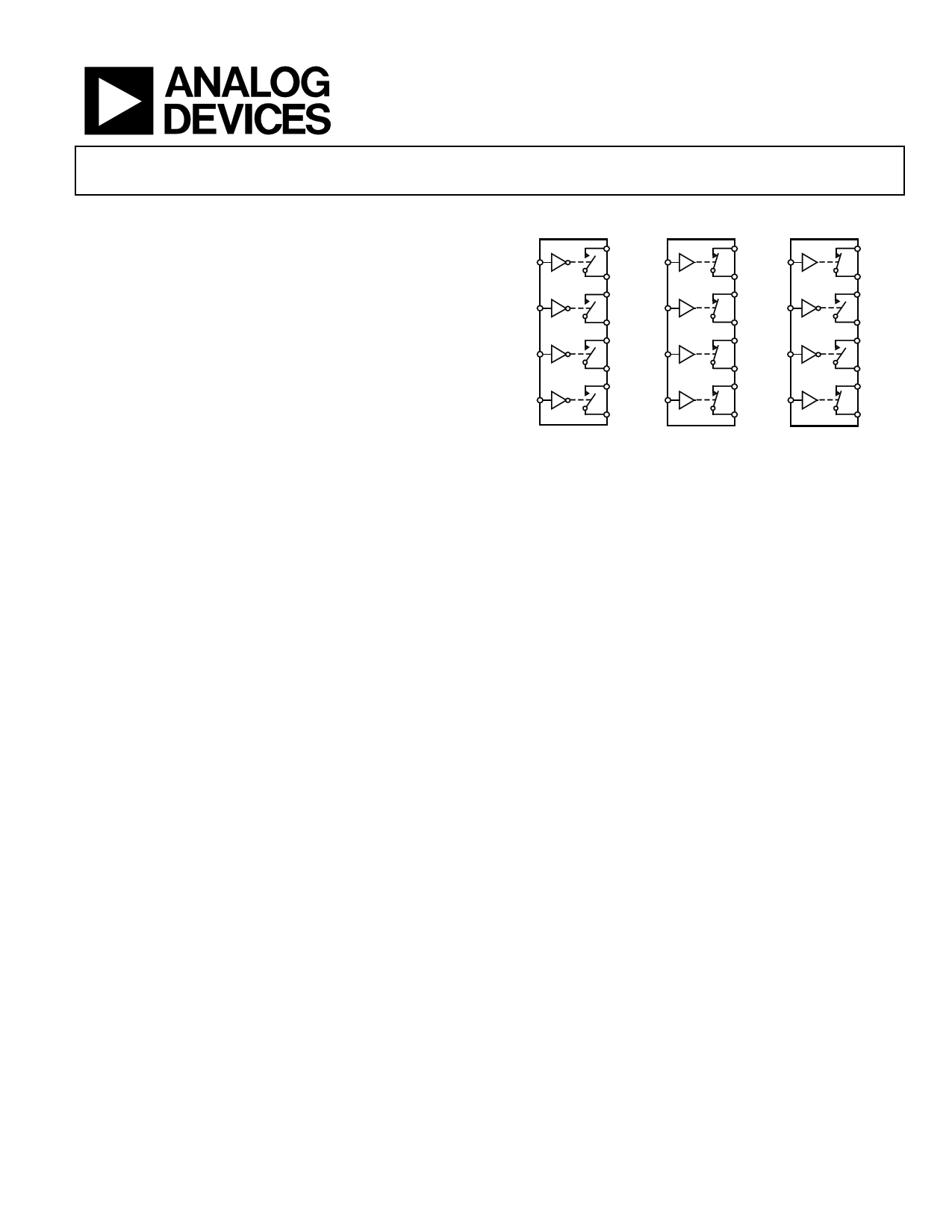
FUNCTIONAL BLOCK DIAGRAM
IN1
IN2
ADG1311
IN3
IN4
S1
D1
S2
D2
S3
D3
S4
D4
IN1
IN2
ADG1312
IN3
IN4
S1
IN1
D1
S1
D1
S2 S2
IN2
D2 D2
ADG1313
S3 S3
IN3
D3 D3
S4
IN4
D4
S4
D4
SWITCHES SHOWN FOR A LOGIC 1 INPUT
Figure 1.
PRODUCT HIGHLIGHTS
1. 3 V logic-compatible digital inputs: VIH = 2.0 V, VIL = 0.8 V.
2. No VL logic power supply required.
3. 16-lead TSSOP and SOIC packages.
Rev. 0
Information furnished by Analog Devices is believed to be accurate and reliable. However, no
responsibility is assumed by Analog Devices for its use, nor for any infringements of patents or other
rights of third parties that may result from its use. Specifications subject to change without notice. No
license is granted by implication or otherwise under any patent or patent rights of Analog Devices.
Trademarksandregisteredtrademarksarethepropertyoftheirrespectiveowners.
One Technology Way, P.O. Box 9106, Norwood, MA 02062-9106, U.S.A.
Tel: 781.329.4700
www.analog.com
Fax: 781.461.3113
© 2005 Analog Devices, Inc. All rights reserved.
1 page 
ABSOLUTE MAXIMUM RATINGS
TA = 25°C, unless otherwise noted.
Table 3.
Parameter
VDD to VSS
VDD to GND
VSS to GND
Analog Inputs1
Digital Inputs1
Peak Current, S or D
Continuous Current per
Channel, S or D
Operating Temperature Range
Automotive
Storage Temperature Range
Junction Temperature
16-Lead TSSOP, θJA Thermal
Impedance (4-layer board)
16-Lead SOIC, θJA Thermal
Impedance
Reflow Soldering Peak
Temperature, Pb free
Rating
35 V
−0.3 V to +25 V
+0.3 V to −25 V
VSS − 0.3 V to VDD + 0.3 V or
30 mA, whichever occurs first
GND − 0.3 V to VDD + 0.3 V or
30 mA, whichever occurs first
100 mA (pulsed at 1 ms,
10% duty cycle max)
25 mA
−40°C to +105°C
−65°C to +150°C
150°C
112°C/W
77°C/W
260°C
1 Overvoltages at IN, S, or D are clamped by internal diodes. Current should be
limited to the maximum ratings given.
ADG1311/ADG1312/ADG1313
Stresses above those listed under Absolute Maximum Ratings
may cause permanent damage to the device. This is a stress
rating only; functional operation of the device at these or any
other conditions above those indicated in the operational
section of this specification is not implied. Exposure to absolute
maximum rating conditions for extended periods may affect
device reliability.
Table 4. ADG1311/ADG1312 Truth Table
ADG1311 INx
ADG1312 INx
Switch Condition
0 1 On
1 0 Off
Table 5. ADG1313 Truth Table
ADG1313 INx
Switch 1, 4
0 Off
1 On
Switch 2, 3
On
Off
ESD CAUTION
ESD (electrostatic discharge) sensitive device. Electrostatic charges as high as 4000 V readily accumulate on
the human body and test equipment and can discharge without detection. Although this product features
proprietary ESD protection circuitry, permanent damage may occur on devices subjected to high energy
electrostatic discharges. Therefore, proper ESD precautions are recommended to avoid performance
degradation or loss of functionality.
Rev. 0 | Page 5 of 12
5 Page 
VDD
0.1μF
VSS
0.1μF
IN
VIN
VDD
VSS
S
D
GND
50Ω
NETWORK
ANALYZER
50Ω
VS
VOUT
RL
50Ω
VOUT
OFF ISOLATION = 20 log VS
Figure 16. Test Circuit 7—Off Isolation
NETWORK
ANALYZER
VOUT
RL
50Ω
VS
VDD
0.1μF
VSS
0.1μF
VDD
S1
S2
VSS
D2
R
50Ω
GND
CHANNEL-TO-CHANNEL CROSSTALK = 20 log
VOUT
VS
Figure 17. Test Circuit 8—Channel-to-Channel Crosstalk
ADG1311/ADG1312/ADG1313
VDD
0.1μF
VSS
0.1μF
IN
VIN
VDD
VSS
S
D
GND
NETWORK
ANALYZER
50Ω
VS
VOUT
RL
50Ω
VOUT WITH SWITCH
INSERTION LOSS = 20 log VOUT WITHOUT SWITCH
Figure 18. Test Circuit 9—Bandwidth
Rev. 0 | Page 11 of 12
11 Page | ||
| Páginas | Total 12 Páginas | |
| PDF Descargar | [ Datasheet ADG1312.PDF ] | |
Hoja de datos destacado
| Número de pieza | Descripción | Fabricantes |
| ADG1311 | (ADG1311 - ADG1313) Quad SPST Switches | Analog Devices |
| ADG1312 | (ADG1311 - ADG1313) Quad SPST Switches | Analog Devices |
| ADG1313 | (ADG1311 - ADG1313) Quad SPST Switches | Analog Devices |
| Número de pieza | Descripción | Fabricantes |
| SLA6805M | High Voltage 3 phase Motor Driver IC. |
Sanken |
| SDC1742 | 12- and 14-Bit Hybrid Synchro / Resolver-to-Digital Converters. |
Analog Devices |
|
DataSheet.es es una pagina web que funciona como un repositorio de manuales o hoja de datos de muchos de los productos más populares, |
| DataSheet.es | 2020 | Privacy Policy | Contacto | Buscar |