|
|
|
PDF ADSP-21365 Data sheet ( Hoja de datos )
| Número de pieza | ADSP-21365 | |
| Descripción | (ADSP-21365 / ADSP-21366) SHARC Processor | |
| Fabricantes | Analog Devices | |
| Logotipo | ||
Hay una vista previa y un enlace de descarga de ADSP-21365 (archivo pdf) en la parte inferior de esta página. Total 30 Páginas | ||
|
No Preview Available !
www.DataSheet4U.com
a
Preliminary Technical Data
SUMMARY
High performance 32-bit/40-bit floating point processor
optimized for high performance automotive audio
processing
Audio decoder and post processor-algorithm support with
32-bit floating-point implementations
Non-volatile memory may be configured to support audio
decoders and post processor-algorithms like PCM, Dolby
Digital EX, Dolby Prologic IIx, DTS 96/24, Neo:6, DTS ES,
MPEG2 AAC, MPEG2 2channel, MP3, and functions like
Bass management, Delay, Speaker equalization, Graphic
equalization, and more. Decoder/post-processor algo-
rithm combination support will vary depending upon the
chip version and the system configurations. Please visit
www.analog.com/SHARC
SHARC® Processor
ADSP-21365/ADSP-21366
Single-Instruction Multiple-Data (SIMD) computational
architecture
On-chip memory—3M bit of on-chip SRAM and a dedicated
4M bit of on-chip mask-programmable ROM
Code compatible with all other members of the SHARC family
The ADSP-21365/6 is available with a 333 MHz core instruc-
tion rate and unique audio centric peripherals such as the
Digital Audio Interface, S/PDIF transceiver, DTCP (Digital
Content Transmission Protocol) available on the ADSP-
21365 only, serial ports, 8-channel asynchronous sample
rate converter, precision clock generators and more. For
complete ordering information, see Ordering Guide on
page 51
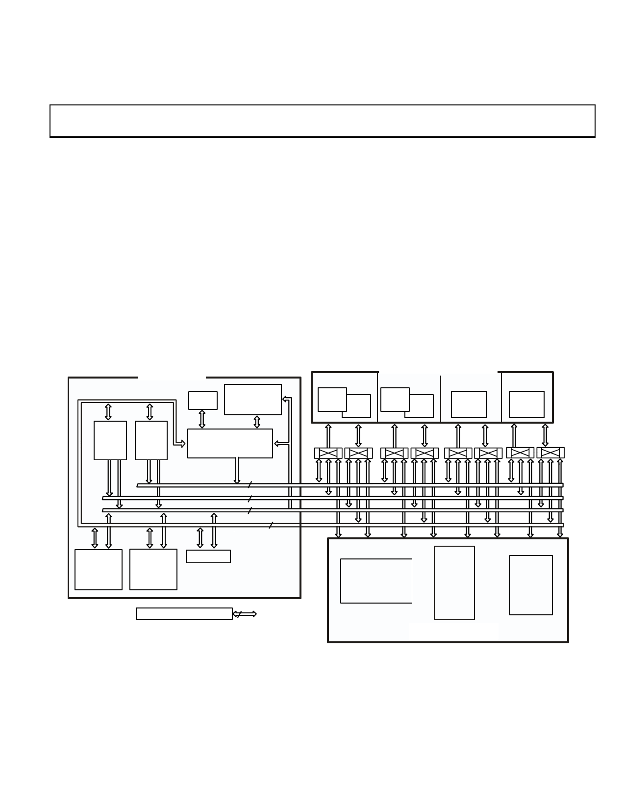
CORE PROCESSOR
TIMER
INSTRUCTION
CACHE
32 X 48-BIT
DAG1
8X4X32
DAG2
8X4X32
PROGRAM
SEQUENCER
BLOCK 0
SRAM
1M BIT ROM
2M BIT
4 BLOCKS OF ON-CHIP MEMORY
BLOCK 1
BLOCK 2
SRAM
1M BIT ROM
2M BIT
SRAM
0.5M BIT
BLOCK 3
SRAM
0.5M BIT
ADDR DATA
ADDR DATA ADDR DATA ADDR DATA
PM ADDRESS BUS
32
DM ADDRESS BUS 32
PM DATA BUS
64
DM DATA BUS 64
IOA IOD
IOA IOD
IOA IOD
IOA IOD
PROCESSING
ELEMENT
(PEX)
PROCESSING
ELEMENT
(PEY)
PX REGISTER
JTAG TEST & EMULATION
6
S
IOP REGISTERS
(MEMORY MAPPED)
SPI
SPORTS
IDP
PCG
TIMERS
SRC
SPDIF
DTCP
I/O PROCESSOR
AND PERIPHERALS
SEE “ADSP-21365/6 MEMORY
AND I/O INTERFACE FEATURES”
SECTION FOR DETAILS
SIGNAL
ROUTING
UNIT
Figure 1. Functional Block Diagram – Processor Core
SHARC and the SHARC logo are registered trademarks of Analog Devices, Inc.
Rev. PrA
Information furnished by Analog Devices is believed to be accurate and reliable.
However, no responsibility is assumed by Analog Devices for its use, nor for any
infringements of patents or other rights of third parties that may result from its use.
Specifications subject to change without notice. No license is granted by implication
or otherwise under any patent or patent rights of Analog Devices. Trademarks and
registered trademarks are the property of their respective companies.
One Technology Way, P.O. Box 9106, Norwood, MA 02062-9106 U.S.A.
Tel:781.329.4700
www.analog.com
Fax:781.326.8703 © 2004 Analog Devices, Inc. All rights reserved.
1 page 
Preliminary Technical Data
ADSP-21365/6
signal processing, and are commonly used in digital filters and
Fourier transforms. The two DAGs of the ADSP-21365/6 con-
tain sufficient registers to allow the creation of up to 32 circular
buffers (16 primary register sets, 16 secondary). The DAGs
automatically handle address pointer wraparound, reduce over-
head, increase performance, and simplify implementation.
Circular buffers can start and end at any memory location.
Flexible Instruction Set
The 48-bit instruction word accommodates a variety of parallel
operations, for concise programming. For example, the
ADSP-21365/6 can conditionally execute a multiply, an add,
and a subtract in both processing elements while branching and
fetching up to four 32-bit values from memory—all in a single
instruction.
ADSP-21365/6 MEMORY AND I/O INTERFACE
FEATURES
The ADSP-21365/6 adds the following architectural features to
the SIMD SHARC family core.
On-Chip Memory
The ADSP-21365/6 contains three megabits of internal SRAM
and four megabits of internal mask-programmable ROM. Each
block can be configured for different combinations of code and
data storage (see Table 2). Each memory block supports single-
cycle, independent accesses by the core processor and I/O pro-
cessor. The ADSP-21365/6 memory architecture, in
combination with its separate on-chip buses, allow two data
transfers from the core and one from the I/O processor, in a sin-
gle cycle.
The ADSP-21365/6’s, SRAM can be configured as a maximum
of 96K words of 32-bit data, 192K words of 16-bit data, 64K
words of 48-bit instructions (or 40-bit data), or combinations of
different word sizes up to three megabits. All of the memory can
be accessed as 16-bit, 32-bit, 48-bit, or 64-bit words. A 16-bit
floating-point storage format is supported that effectively dou-
bles the amount of data that may be stored on-chip. Conversion
between the 32-bit floating-point and 16-bit floating-point for-
mats is performed in a single instruction. While each memory
block can store combinations of code and data, accesses are
most efficient when one block stores data using the DM bus for
transfers, and the other block stores instructions and data using
the PM bus for transfers.
Table 2. ADSP-21365/6 Internal Memory Space
IOP Registers 0x0000 0000 - 0003 FFFF
Long Word (64 bits)
Extended Precision Normal or Normal Word (32 bits)
Instruction Word (48 bits)
BLOCK 0 ROM
0x0004 0000–0x0004 7FFF
BLOCK 0 ROM
0x0008 0000–0x0008 AAAA
BLOCK 0 ROM
0x0008 0000–0x0008 FFFF
Reserved
0x0004 8000–0x0004 BFFF
Reserved
0x0009 0000–0x0009 7FFF
BLOCK 0 RAM
0x0004 C000–0x0004 FFFF
BLOCK 0 RAM
0x0009 0000–0x0009 5555
BLOCK 0 RAM
0x0009 8000–0x0009 FFFF
BLOCK 1 ROM
0x0005 0000–0x0005 7FFF
BLOCK 1 ROM
0x000A 0000–0x000A AAAA
BLOCK 1 ROM
0x000A 0000– 0x000A FFFF
Reserved
0x0005 8000–0x0005 BFFF
Reserved
0x000B 0000– 0x000B 7FFF
BLOCK 1 RAM
0x0005 C000–0x0005 FFFF
BLOCK 1 RAM
0x000B 0000–0x000B 5555
BLOCK 1 RAM
0x000B 8000–0x000B FFFF
BLOCK 2 RAM
0x0006 0000–0x0006 1FFF
BLOCK 2 RAM
0x000C 0000–0x000C 2AAA
BLOCK 2 RAM
0x000C 0000–0x000C 3FFF
Reserved
0x0006 2000– 0x0006 FFFF
Reserved
0x000C 4000– 0x000D FFFF
BLOCK 3 RAM
0x0007 0000–0x0007 1FFF
BLOCK 3 RAM
0x000E 0000–0x000E 2AAA
BLOCK 3 RAM
0x000E 0000–0x000E 3FFF
Reserved
0x0007 2000– 0x0007 FFFF
Reserved
0x000E 4000–0x000F FFFF
Short Word (16 bits)
BLOCK 0 ROM
0x0010 0000–0x0011 FFFF
Reserved
0x0012 0000–0x0012 FFFF
BLOCK 0 RAM
0x0013 0000–0x0013 FFFF
BLOCK 1 ROM
0x0014 0000–0x0015 FFFF
Reserved
0x0016 0000–0x0016 FFFF
BLOCK 1 RAM
0x0017 0000–0x0017 FFFF
BLOCK 2 RAM
0x0018 0000–0x0018 7FFF
Reserved
0x0018 8000–0x001B FFFF
BLOCK 3 RAM
0x001C 0000–0x001C 7FFF
Reserved
0x001C 8000–0x001F FFFF
Reserved
0x0020 0000–0xFFFF FFFF
Rev. PrA | Page 5 of 54 | September 2004
5 Page 
Preliminary Technical Data
ADSP-21365/6
PIN FUNCTION DESCRIPTIONS
ADSP-21365/6 pin definitions are listed below. Inputs identified
as synchronous (S) must meet timing requirements with respect
to CLKIN (or with respect to TCK for TMS and TDI). Inputs
identified as asynchronous (A) can be asserted asynchronously
to CLKIN (or to TCK for TRST). Tie or pull unused inputs to
VDDEXT or GND, except for the following:
• DAI_Px, SPICLK, MISO, MOSI, EMU, TMS, TRST, TDI,
and AD15–0 (NOTE: These pins have pullup resistors.)
The following symbols appear in the Type column of Table 3:
A = Asynchronous, G = Ground, I = Input, O = Output,
P = Power Supply, S = Synchronous, (A/D) = Active Drive,
(O/D) = Open Drain, and T = Three-State , (pd) = pulldown
resistor, (pu) = pullup resistor.
Table 3. Pin Descriptions
Pin Type
AD15–0
I/O/T
(pu)
RD
WR
ALE
FLAG3–0
O
(pu)
O
(pu)
O
(pd)
I/O/A
State During and
After Reset
Three-state with
pullup enabled
Three-state, driven
high1
Three-state, driven
high1
Three-state, driven
low1
Three-state
Function
Parallel Port Address/Data. The ADSP-21365/6 parallel port and its corresponding
DMA unit output addresses and data for peripherals on these multiplexed pins. The
multiplex state is determined by the ALE pin. The parallel port can operate in either
8-bit or 16-bit mode. Each AD pin has a 22.5 kΩ internal pullup resistor. See Address
Data Modes on page 14 for details of the AD pin operation.
For 8-bit mode: ALE is automatically asserted whenever a change occurs in the upper
16 external address bits, A23–8; ALE is used in conjunction with an external latch to
retain the values of the A23–8.
For 16-bit mode: ALE is automatically asserted whenever a change occurs in the
address bits, A15–0; ALE is used in conjunction with an external latch to retain the
values of the A15–0. To use these pins as flags (FLAGS15–0) or PWMs (PWM15–0), 1)
set (=1) bit 20 of the SYSCTL register to disable the parallel port, 2) set (=1) bits 22–25
of the SYSCTL register to enable FLAGS in groups of four (bit 22 for FLAGS3–0, bit 23
for FLAGS7–4 etc.) or, set (=1) bits 26–29 of the SYSCTL register to enable PWMs in
groups of four (bit 26 for PWM0–3, bit 27 for PWM4–7, and so on). When used as an
input, the IDP Channel 0 can use these pins for parallel input data.
Parallel Port Read Enable. RD is asserted low whenever the processor reads 8-bit or
16-bit data from an external memory device. When AD15–0 are flags, this pin remains
deasserted. RD has a 22.5 kΩ internal pullup resistor.
Parallel Port Write Enable. WR is asserted low whenever the processor writes 8-bit or
16-bit data to an external memory device. When AD15–0 are flags, this pin remains
deasserted. WR has a 22.5 kΩ internal pullup resistor.
Parallel Port Address Latch Enable. ALE is asserted whenever the processor drives
a new address on the parallel port address pins. On reset, ALE is active high. However,
it can be reconfigured using software to be active low. When AD15–0 are flags, this
pin remains deasserted. ALE has a 20 kΩ internal pulldown resistor.
Flag Pins. Each flag pin is configured via control bits as either an input or output. As
an input, it can be tested as a condition. As an output, it can be used to signal external
peripherals. These pins can be used as an SPI interface slave select output during SPI
mastering. These pins are also multiplexed with the IRQx and the TIMEXP signals.
In SPI master boot mode, FLAG0 is the slave select pin that must be connected to an
SPI EPROM. FLAG0 is configured as a slave select during SPI master boot. When bit 16
is set (=1) in the SYSCTL register, FLAG0 is configured as IRQ0.
When bit 17 is set (=1) in the SYSCTL register, FLAG1 is configured as IRQ1.
When bit 18 is set (=1) in the SYSCTL register, FLAG2 is configured as IRQ2.
When bit 19 is set (=1) in the SYSCTL register, FLAG3 is configured as TIMEXP which
indicates that the system timer has expired.
Rev. PrA | Page 11 of 54 | September 2004
11 Page | ||
| Páginas | Total 30 Páginas | |
| PDF Descargar | [ Datasheet ADSP-21365.PDF ] | |
Hoja de datos destacado
| Número de pieza | Descripción | Fabricantes |
| ADSP-21362 | (ADSP-21362 - ADSP-21366) SHARC Processor | Analog Devices |
| ADSP-21363 | SHARC Processor | Analog Devices |
| ADSP-21363 | (ADSP-21362 - ADSP-21366) SHARC Processor | Analog Devices |
| ADSP-21364 | SHARC Processor | Analog Devices |
| Número de pieza | Descripción | Fabricantes |
| SLA6805M | High Voltage 3 phase Motor Driver IC. |
Sanken |
| SDC1742 | 12- and 14-Bit Hybrid Synchro / Resolver-to-Digital Converters. |
Analog Devices |
|
DataSheet.es es una pagina web que funciona como un repositorio de manuales o hoja de datos de muchos de los productos más populares, |
| DataSheet.es | 2020 | Privacy Policy | Contacto | Buscar |