|
|
|
PDF ADL5391 Data sheet ( Hoja de datos )
| Número de pieza | ADL5391 | |
| Descripción | DC to 2.0 GHz Multiplier | |
| Fabricantes | Analog Devices | |
| Logotipo | ||
Hay una vista previa y un enlace de descarga de ADL5391 (archivo pdf) en la parte inferior de esta página. Total 16 Páginas | ||
|
No Preview Available !
www.DataSheet4U.com
FEATURES
Ultrafast symmetric multiplier
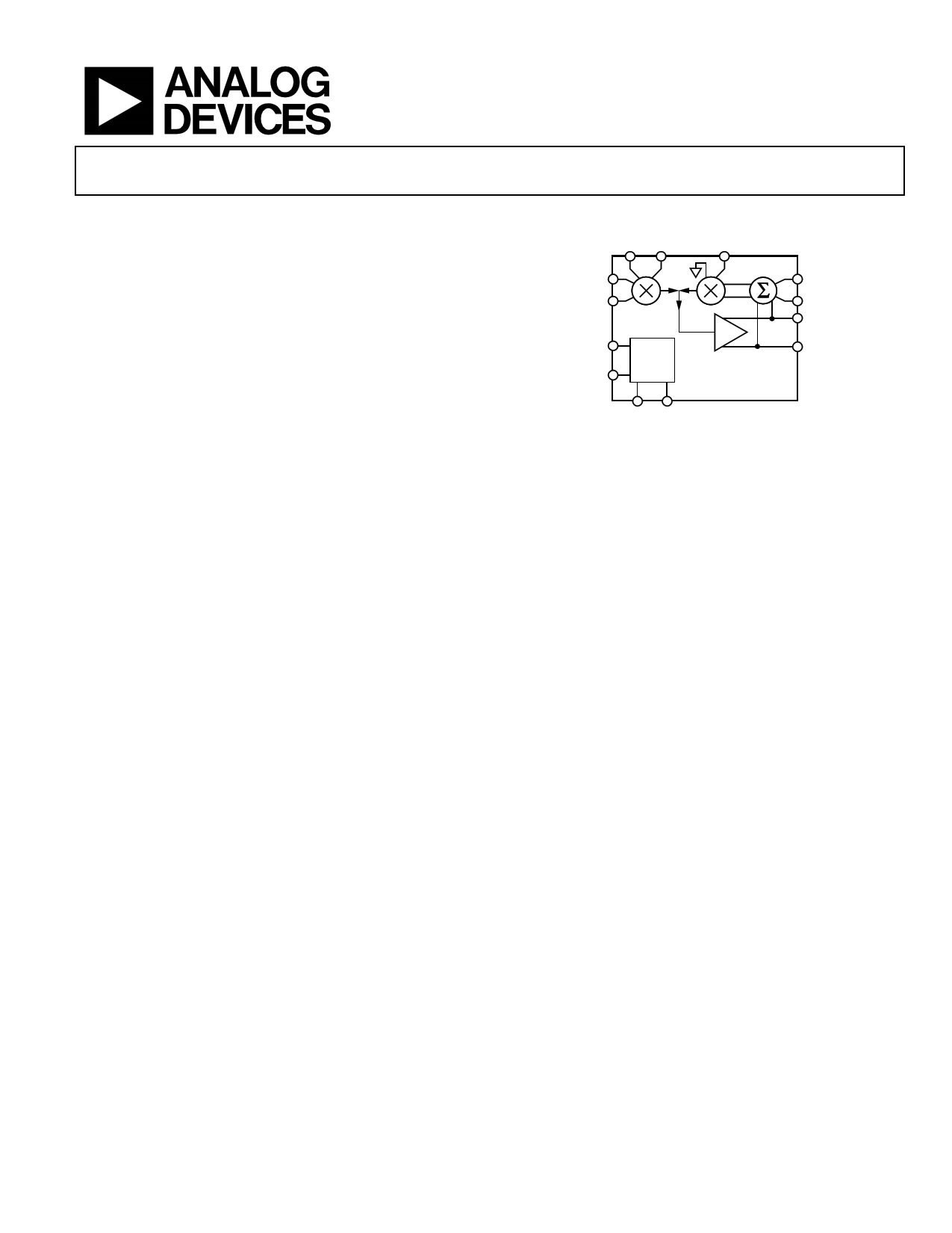
Function: VW = α × (VX × VY)/1 V + VZ
Unique design ensures absolute XY-symmetry
Identical X and Y amplitude/timing responses
Adjustable gain scaling, α
DC-coupled throughout, 3 dB bandwidth of 2 GHz
Fully differential inputs, may be used single ended
Low noise, high linearity
Accurate, temperature stable gain scaling
Single-supply operation (4.5 V to 5.5 V @ 130 mA)
Low current power-down mode
16-lead LFCSP
APPLICATIONS
Wideband multiplication and summing
High frequency analog modulation
Adaptive antennas (diversity/phased array)
Square-law detectors and true rms detectors
Accurate polynomial function synthesis
DC capable VGA with very fast control
GENERAL DESCRIPTION
The ADL5391 draws on three decades of experience in
advanced analog multiplier products. It provides the same
general mathematical function that has been field proven to
provide an exceptional degree of versatility in function synthesis.
VW = α × (VX × VY)/ 1 V + VZ
The most significant advance in the ADL5391 is the use of a
new multiplier core architecture, which differs markedly from
the conventional form that has been in use since 1970. The
conventional structure that employs a current mode, translinear
core is fundamentally asymmetric with respect to the X and Y
inputs, leading to relative amplitude and timing misalignments
that are problematic at high frequencies. The new multiplier
core eliminates these misalignments by offering symmetric
signal paths for both X and Y inputs. The Z input allows a signal
to be added directly to the output. This can be used to cancel a
carrier or to apply a static offset voltage.
The fully differential X, Y, and Z input interfaces are operational
over a ±2 V range, and they can be used in single-ended fashion.
The user can apply a common mode at these inputs to vary
from the internally set VPOS/2 down to ground. If these inputs
Rev. 0
Information furnished by Analog Devices is believed to be accurate and reliable. However, no
responsibility is assumed by Analog Devices for its use, nor for any infringements of patents or other
rights of third parties that may result from its use. Specifications subject to change without notice. No
license is granted by implication or otherwise under any patent or patent rights of Analog Devices.
Trademarksandregisteredtrademarksarethepropertyoftheirrespectiveowners.
DC to 2.0 GHz
Multiplier
ADL5391
FUNCTIONAL BLOCK DIAGRAM
YMNS YPLS
GADJ
XPLS
XMNS
ENBL
VMID
ADL5391
W = αXY/1V+Z
COMM VPOS
Figure 1.
ZMNS
ZPLS
WPLS
WMNS
are ac-coupled, their nominal voltage will be VPOS/2. These input
interfaces each present a differential 500 Ω input impedance up to
approximately 700 MHz, decreasing to 50 Ω at 2 GHz. The gain
scaling input, GADJ, can be used for fine adjustment of the gain
scaling constant (α) about unity.
The differential output can swing ±2 V about the VPOS/2
common-mode and can be taken in a single-ended fashion as
well. The output common mode is designed to interface directly
to the inputs of another ADL5391. Light dc loads can be ground
referenced; however, ac-coupling of the outputs is recommended
for heavy loads.
The ENBL pin allows the ADL5391 to be disabled quickly to a
standby mode. It operates off supply voltages from 4.5 V to
5.5 V while consuming approximately 130 mA.
The ADL5391 is fabricated on Analog Devices proprietary, high
performance, 65 GHz, SOI complementary, SiGe bipolar IC
process. It is available in a 16-lead, Pb-free, LFCSP and operates
over a −40°C to +85°C temperature range. Evaluation boards
are available.
One Technology Way, P.O. Box 9106, Norwood, MA 02062-9106, U.S.A.
Tel: 781.329.4700
www.analog.com
Fax: 781.461.3113
©2006 Analog Devices, Inc. All rights reserved.
1 page 
ABSOLUTE MAXIMUM RATINGS
Table 2.
Parameter
Supply Voltage VPOS
ENBL
XPLS, XMNS, YPLS, YMNS, ZPLS, ZMNS
GADJ
Internal Power Dissipation
θJA (With Pad Soldered to Board)
Maximum Junction Temperature
Operating Temperature Range
Storage Temperature Range
Lead Temperature (Soldering 60 sec)
Rating
5.5 V
5.5 V
VPOS
VPOS
800 mW
73°C/W
150°C
−40°C to +85°C
−65°C to +150°C
300°C
ADL5391
Stresses above those listed under Absolute Maximum Ratings
may cause permanent damage to the device. This is a stress
rating only; functional operation of the device at these or any
other conditions above those indicated in the operational
section of this specification is not implied. Exposure to absolute
maximum rating conditions for extended periods may affect
device reliability.
ESD CAUTION
ESD (electrostatic discharge) sensitive device. Electrostatic charges as high as 4000 V readily accumulate on the
human body and test equipment and can discharge without detection. Although this product features
proprietary ESD protection circuitry, permanent damage may occur on devices subjected to high energy
electrostatic discharges. Therefore, proper ESD precautions are recommended to avoid performance
degradation or loss of functionality.
Rev. 0 | Page 5 of 16
5 Page 
Matching the Input/Output
The input and output impedance’s of the ADL5391 change over
frequency, making it difficult to match over a broad frequency
range (see Figure 15 and Figure 16). The evaluation board is
matched for lower frequency operation, and the impedance
change at higher frequencies causes the change in gain seen in
Figure 6. If desired, the user of the ADL5391 can design a
matching network to fit their application.
Wideband Voltage-Controlled Amplifier/Amplitude
Modulator
Most of the data for the ADL5391 was collected by using it as a
fast reacting analog VGA. Either X or Y inputs can be used for
the RF input (and the other as the very fast analog control),
because either input can be used from dc to 2 GHz. There is a
linear relationship between the analog control and the output of
the multiplier in the VGA mode. Figure 6 and Figure 7 show the
dynamic range available in VGA mode (without optimizing the
dc offsets).
The speed of the ADL5391 in VGA mode allows it to be used as
an amplitude modulator. Either or both inputs can have
modulation or CW applied. AM modulation is achieved by
feeding CW into X (or Y) and adding AM modulation to the Y
(or X) input.
Squaring and Frequency Doubling
Amplitude domain squaring of an input signal, E, is achieved
simply by connecting the X and Y inputs in parallel to produce
an output of E2. The input can be single-ended, differential, or
through a balun (frequency range and dynamic range can be
limited if used single ended).
When the input is a sine wave Esin(ωt), a signal squarer behaves
as a frequency doubler, because
[Esin(ωt)]2 = E 2 (1− cos(2ωt ))
2
(3)
Ideally, when used for squaring and frequency doubling, there is
no component of the original signals on the output. Because of
internal offsets, this is not the case. If Equation 3 were rewritten
to include theses offsets, it could separate into three output
terms (Equation 4).
[ ]Esin(ωt) + OFST ×[Esin(ωt) + OFST] =
E2
2
[cos(2ωt)]+
2 Esin(ωt )OFST
+
⎜⎜⎝⎛OFST 2
+
E2
2
⎟⎟⎠⎞
(4)
where:
The dc component is OFST2 + E2/2.
The input signal bleedthrough is 2Esin(ωt)OFST.
The input squared is E2/2[cos(2ωt)].
ADL5391
The dc component of the output is related to the square of both
the offset (OFST) and the signal input amplitude (E). The offset
can be found in Figure 4 and is approximately 20 mV. The
second harmonic output grows with the square of the input
amplitude, and the signal bleedthrough grows proportionally
with the input signal. For smaller signal amplitudes, the signal
bleedthrough can be higher than the second harmonic
component. As the input amplitude increases, the second
harmonic component grows much faster than the signal
bleedthrough and becomes the dominant signal at the output.
If the X and Y inputs are driven too hard, third harmonic
components will also increase.
For best performance creating harmonics, the ADL5391 should
be driven differentially. Figure 17 shows the performance of the
ADL5391 when used as a harmonic generator (the evaluation
board was used with R9 and R10 removed and R2 = 56.2 Ω). If
dc operation is necessary, the ADL5391 can be driven single
ended (without the dc blocks). The flatness of the response over
a broad frequency range depends on the input/output match.
The fundamental bleed through not only depends on the
amount of power put into the device but also depends on
matching the unused differential input/output to the same
impedance as the used input/output. Figure 18 shows the
performance of the ADL5391 when driven single ended
(without ac coupling capacitors), and Figure 19 shows the
schematic of the setup. A resistive input/output match were
used to match the input from dc to 1 GHz and the output from
dc to 2 GHz. Reactive matching can be used for more narrow
frequency ranges. When matching the input/output of the
ADL5391, care needs to be taken not to load the ADL5391 too
heavily; the maximum reference current available is 50 mA.
–15
–20
SECOND HARMONIC GAIN
–25
–30
–35 BLEEDTHRU GAIN
–40
–45
–50
–55
–60 THIRD HARMONIC GAIN
–65
10
100 200 300 400 500 600 700 800 900 1000
FREQUENCY (MHz)
Figure 17. ADL5391 Used as a Harmonic Generator
Rev. 0 | Page 11 of 16
11 Page | ||
| Páginas | Total 16 Páginas | |
| PDF Descargar | [ Datasheet ADL5391.PDF ] | |
Hoja de datos destacado
| Número de pieza | Descripción | Fabricantes |
| ADL5390 | RF/IF Vector Multiplier | Analog Devices |
| ADL5391 | DC to 2.0 GHz Multiplier | Analog Devices |
| Número de pieza | Descripción | Fabricantes |
| SLA6805M | High Voltage 3 phase Motor Driver IC. |
Sanken |
| SDC1742 | 12- and 14-Bit Hybrid Synchro / Resolver-to-Digital Converters. |
Analog Devices |
|
DataSheet.es es una pagina web que funciona como un repositorio de manuales o hoja de datos de muchos de los productos más populares, |
| DataSheet.es | 2020 | Privacy Policy | Contacto | Buscar |