|
|
|
PDF ADA4310-1 Data sheet ( Hoja de datos )
| Número de pieza | ADA4310-1 | |
| Descripción | High Current Output Line Driver | |
| Fabricantes | Analog Devices | |
| Logotipo | ||
Hay una vista previa y un enlace de descarga de ADA4310-1 (archivo pdf) en la parte inferior de esta página. Total 15 Páginas | ||
|
No Preview Available !
Data Sheet
Low Cost, Dual, High Current Output
Line Driver with Shutdown
ADA4310-1
FEATURES
High speed
−3 dB bandwidth: 190 MHz, G = +5
Slew rate: 820 V/µs, RLOAD = 50 Ω
Wide output swing
20.4 V p-p differential, RLOAD of 100 Ω from 12 V supply
High output current
Low distortion
−95 dBc typical at 1 MHz, VOUT = 2 V p-p, G = +5, RLOAD = 50 Ω
−69 dBc typical at 10 MHz, VOUT = 2 V p-p, G = +5, RLOAD = 50 Ω
Power management and shutdown
Control inputs CMOS level compatible
Shutdown quiescent current 0.65 mA/amplifier
Adjustable low quiescent current: 3.9 mA to 7.6 mA per amp
APPLICATIONS
Home networking line drivers
Twisted pair line drivers
Power line communications
Video line drivers
ARB line drivers
I/Q channel amplifiers
PIN CONFIGURATIONS
ADA4310-1
+VS 1
NIC 2
OUT A 3
–IN A 4
+IN A 5
10 OUT B
9 –IN B
8 +IN B
7 PD1
6 PD0
NOTES
1. THE EXPOSED PAD MUST BE CONNECTED
TO GROUND (ELECTRICAL CONNECTION REQUIRED).
2. NIC = NO INTERNAL CONNECTION.
Figure 1. Thermally Enhanced, 10-Lead MINI_SO_EP
NIC 1
−IN A 2
+IN A 3
GND 4
ADA4310-1
12 NIC
11 −IN B
10 +IN B
9 PD1
NOTES
1. NIC = NO INTERNAL CONNECTION.
2. THE EXPOSED PAD MUST BE
CONNECTED TO GND.
Figure 2. Thermally Enhanced, 4 mm × 4 mm 16-Lead LFCSP
GENERAL DESCRIPTION
The ADA4310-1 is comprised of two high speed, current
feedback operational amplifiers. The high output current, high
bandwidth, and fast slew rate make it an excellent choice for
broadband applications requiring high linearity performance
while driving low impedance loads.
The ADA4310-1 incorporates a power management function
that provides shutdown capabilities and/or the ability to
optimize the amplifiers quiescent current. The CMOS-
compatible, power-down control pins (PD1 and PD0) enable
the ADA4310-1 to operate in four different modes: full power,
medium power, low power, and complete power down. In the
power-down mode, quiescent current drops to only
0.65 mA/amplifier, while the amplifier output goes to a high
impedance state.
The ADA4310-1 is available in a thermally enhanced, 10-lead
MSOP with an exposed paddle for improved thermal conduction
and in a thermally enhanced, 4 mm × 4 mm 16-lead LFCSP.
The ADA4310-1 is rated to work in the extended industrial
temperature range of −40°C to +85°C.
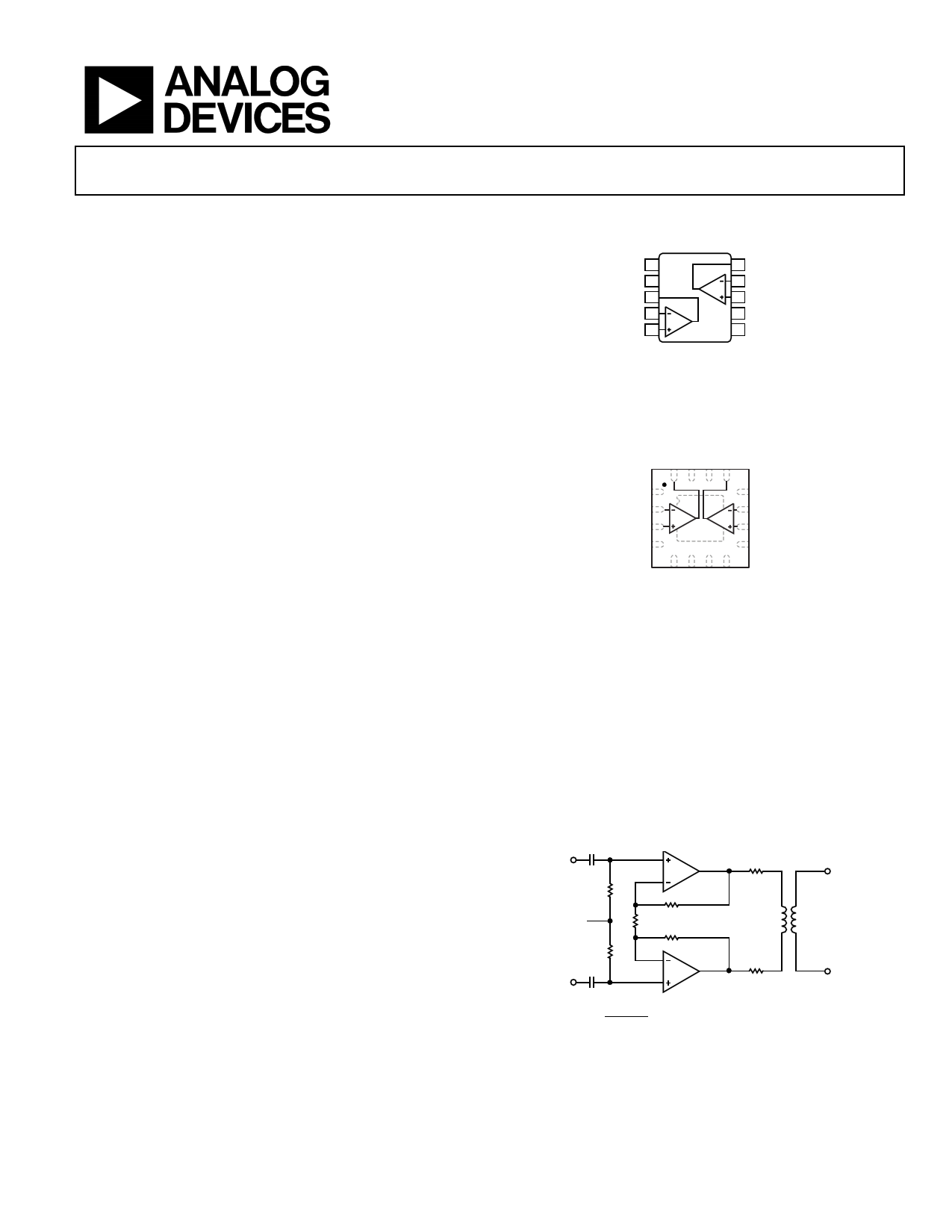
VMID1
1/2
ADA4310-1
1/2
1VMID =
VCC – VEE
2
ADA4310-1
Figure 3. Typical PLC Driver Application
Rev. B
Document Feedback
Information furnished by Analog Devices is believed to be accurate and reliable. However, no
responsibilityisassumedbyAnalogDevices for itsuse,nor foranyinfringementsofpatentsor other
rights of third parties that may result from its use. Specifications subject to change without notice. No
license is granted by implication or otherwise under any patent or patent rights of Analog Devices.
Trademarksandregisteredtrademarksarethepropertyoftheirrespectiveowners.
One Technology Way, P.O. Box 9106, Norwood, MA 02062-9106, U.S.A.
Tel: 781.329.4700 ©2006–2016 Analog Devices, Inc. All rights reserved.
Technical Support
www.analog.com
1 page 
ADA4310-1
Parameter
POWER DOWN PINS
PD1, PD0 Threshold
PD1, PD0 = 0 Pin Bias Current
PD1, PD0 = 1 Pin Bias Current
Enable/Disable Time
Power Supply Rejection Ratio
Test Conditions/Comments
Referenced to GND
PD1 or PD0 = 0 V
PD1 or PD0 = 3 V
Positive/Negative
Data Sheet
Min Typ
Max Unit
1.5
−0.2
70
−70/−60
0.04/2
V
µA
µA
µs
dB
Rev. B | Page 4 of 14
5 Page 
ADA4310-1
THEORY OF OPERATION
The ADA4310-1 is a current feedback amplifier with high
output current capability. With a current feedback amplifier, the
current into the inverting input is the feedback signal, and the
open-loop behavior is that of a transimpedance, dVO/dIIN or TZ.
The open-loop transimpedance is analogous to the open-loop
voltage gain of a voltage feedback amplifier. Figure 20 shows a
simplified model of a current feedback amplifier. Because RIN is
proportional to 1/gm, the equivalent voltage gain is just TZ × gm,
where gm is the transconductance of the input stage. Basic
analysis of the follower with gain circuit yields
VO
VIN
G
TZ
s
TZ s
G RIN
RF
where:
G 1 RF
RG
RIN
1
gm
50 Ω
Data Sheet
Because G × RIN << RF for low gains, a current feedback
amplifier has relatively constant bandwidth vs. gain, the 3 dB
point being set when |TZ| = RF.
Of course, for a real amplifier there are additional poles that
contribute excess phase, and there is a value for RF below which
the amplifier is unstable. Tolerance for peaking and desired
flatness determines the optimum RF in each application.
RF
RG
RN
VIN
RIN
IIN TZ
VOUT
Figure 20. Simplified Block Diagram
Rev. B | Page 10 of 14
11 Page | ||
| Páginas | Total 15 Páginas | |
| PDF Descargar | [ Datasheet ADA4310-1.PDF ] | |
Hoja de datos destacado
| Número de pieza | Descripción | Fabricantes |
| ADA4310-1 | High Current Output Line Driver | Analog Devices |
| Número de pieza | Descripción | Fabricantes |
| SLA6805M | High Voltage 3 phase Motor Driver IC. |
Sanken |
| SDC1742 | 12- and 14-Bit Hybrid Synchro / Resolver-to-Digital Converters. |
Analog Devices |
|
DataSheet.es es una pagina web que funciona como un repositorio de manuales o hoja de datos de muchos de los productos más populares, |
| DataSheet.es | 2020 | Privacy Policy | Contacto | Buscar |