|
|
|
PDF AD8392 Data sheet ( Hoja de datos )
| Número de pieza | AD8392 | |
| Descripción | Dual-Channel ADSL/ADSL2+ Line Driver | |
| Fabricantes | Analog Devices | |
| Logotipo | ||
Hay una vista previa y un enlace de descarga de AD8392 (archivo pdf) en la parte inferior de esta página. Total 16 Páginas | ||
|
No Preview Available !
Low Power, High Output Current, Quad Op Amp,
Dual-Channel ADSL/ADSL2+ Line Driver
AD8392
FEATURES
Four current feedback, high current amplifiers
Ideal for use as ADSL/ADSL2+ dual-channel Central Office
(CO) line drivers
Low power operation
Power supply operation from ±5 V (+10 V) up to ±12 V (+24 V)
Less than 3 mA/Amp quiescent supply current for full
power ADSL/ADSL2+ CO applications (20.4 dBm line
power, 5.5 CF)
Three active power modes plus shutdown
High output voltage and current drive
400 mA peak output drive current
44 V p-p differential output voltage
Low distortion
−72 dBc @1 MHz second harmonic
−82 dBc @ 1 MHz third harmonic
High speed: 900 V/µs differential slew rate
Additional functionality of AD8392ACP
On-chip common-mode voltage generation
APPLICATIONS
ADSL/ADSL2+ CO line drivers
XDSL line drives
High output current, low distortion amplifiers
DAC output buffer
GENERAL DESCRIPTION
The AD8392 is comprised of four high output current, low
power consumption, operational amplifiers. It is particularly
well suited for the CO driver interface in digital subscriber line
systems, such as ADSL and ADSL2+. The driver is capable of
providing enough power to deliver 20.4 dBm to a line, while
compensating for losses due to hybrid insertion and back
termination resistors. In addition, the low distortion, fast slew
rate, and high output current capability make the AD8392 ideal
for many other applications, including medical instrumenta-
tion, DAC output drivers, and other high peak current circuits.
The AD8392 is available in two thermally enhanced packages, a
28-lead TSSOP/EP (AD8392ARE) and a 5 mm × 5 mm 32-lead
LFCSP (AD8392ACP). Four bias modes are available via the use
of two digital bits (PD1, PD0).
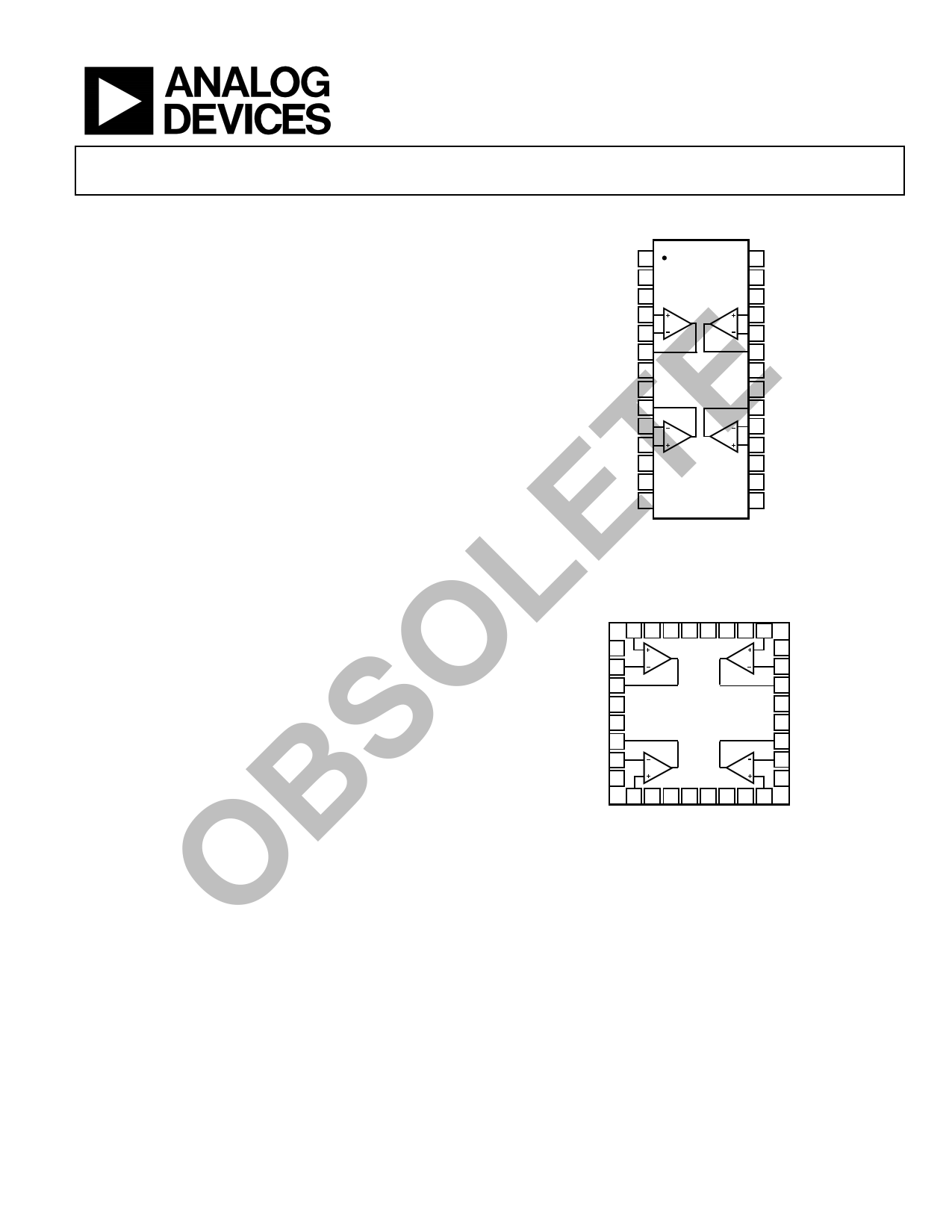
PIN CONFIGURATIONS
VEE 1
PD0 1, 2 2
PD1 1, 2 3
+VIN1
–VIN1
VOUT1
VCC
4
5
6
7
NC 8
VOUT3 9
–VIN3 10
+VIN3 11
NC 12
NC 13
GND 14
12
AD8392
34
28 GND
27 NC
26 NC
25 +VIN2
24 –VIN2
23 VOUT2
22 NC
21 VCC
20 VOUT4
19 –VIN4
18 +VIN4
17 PD1 3, 4
16 PD0 3, 4
15 VEE
NC = NO CONNECT
Figure 1. AD8392ARE, 28-Lead TSSOP/EP
32 31 30 29 28 27 26 25
NC 1
–VIN1 2
VOUT1 3
VCC 4
NC 5
VOUT3 6
–VIN3 7
NC 8
12
AD8392
34
24 NC
23 –VIN2
22 VOUT2
21 NC
20 VCC
19 VOUT4
18 –VIN4
17 NC
9 10 11 12 13 14 15 16
NC = NO CONNECT
Figure 2. AD8392ACP, 32-Lead LFCSP 5 mm × 5 mm
Additionally, the AD8392ACP provides VCOM pins for on-chip
common mode voltage generation.
The low power consumption, high output current, high output
voltage swing, and robust thermal packaging enable the
AD8392 to be used as the CO line drivers in ADSL and other
xDSL systems, as well as other high current, single-ended or
differential amplifier applications.
Rev. A
Information furnished by Analog Devices is believed to be accurate and reliable.
However, no responsibility is assumed by Analog Devices for its use, nor for any
infringements of patents or other rights of third parties that may result from its use.
Specifications subject to change without notice. No license is granted by implication
or otherwise under any patent or patent rights of Analog Devices. Trademarks and
registered trademarks are the property of their respective owners.
One Technology Way, P.O. Box 9106, Norwood, MA 02062-9106, U.S.A.
Tel: 781.329.4700
www.analog.com
Fax: 781.461.3113
©2005 Analog Devices, Inc. All rights reserved.
1 page 
ABSOLUTE MAXIMUM RATINGS
Table 3.
Parameter
Supply Voltage
Power Dissipation
Storage Temperature
Operating Temperature Range
Lead Temperature Range (Soldering 10 sec)
Junction Temperature
Rating
±13 V (+26 V)
See Figure 3
−65°C to +150°C
−40°C to +85°C
300°C
150°C
Stresses above those listed under Absolute Maximum Ratings
may cause permanent damage to the device. This is a stress
rating only; functional operation of the device at these or any
other conditions above those indicated in the operational
section of this specification is not implied. Exposure to absolute
maximum rating conditions for extended periods may affect
device reliability.
THERMAL RESISTANCE
θJA is specified for the worst-case conditions, i.e., θJA is specified
for device soldered in circuit board for surface-mount packages.
Table 4. Thermal Resistance
Package Type
LFCSP-32 (CP)
TSSOP-28/EP (RE)
θJA
27.27
35.33
Unit
°C/W
°C/W
Maximum Power Dissipation
The power dissipated in the package (PD) is the sum of the
quiescent power dissipation and the power dissipated in the
package due to the load drive for all outputs. The quiescent
power is the voltage between the supply pins (VS) times the
quiescent current (IS). Assuming that the load (RL) is midsupply,
the total drive power is VS/2 × IOUT, some of which is
dissipated in the package and some in the load (VOUT × IOUT).
AD8392
RMS output voltages should be considered. If RL is referenced
to VS− as in single-supply operation, the total power is VS × IOUT.
In single supply with RL to VS−, worst case is VOUT = VS/2.
Airflow increases heat dissipation, effectively reducing θJA. Also,
more metal directly in contact with the package leads from
metal traces, through holes, ground, and power planes reduces
the θJA.
Figure 3 shows the maximum safe power dissipation in the
package versus the ambient temperature for the LFCSP-32 and
TSSOP-28/EP packages on a JEDEC standard 4-layer board. θJA
values are approximations.
7
TJ = 150°C
6
5
LFCSP-32
4
TSSOP-28/EP
3
2
1
0
–40 –30 –20 –10 0 10 20 30 40 50 60 70 80 90
TEMPERATURE (°C)
Figure 3. Maximum Power Dissipation vs. Temperature for a 4-Layer Board
See the Thermal Considerations section for additional thermal
design guidance.
ESD CAUTION
ESD (electrostatic discharge) sensitive device. Electrostatic charges as high as 4000 V readily accumulate on the
human body and test equipment and can discharge without detection. Although this product features proprie-
tary ESD protection circuitry, permanent damage may occur on devices subjected to high energy electrostatic
discharges. Therefore, proper ESD precautions are recommended to avoid performance degradation or loss of
functionality.
Rev. A | Page 5 of 16
5 Page 
THEORY OF OPERATION
The AD8392 is a current feedback amplifier with high
(400 mA) output current capability. With a current feedback
amplifier, the current into the inverting input is the feedback
signal, and the open-loop behavior is that of a transimpedance,
dVO/dIIN or TZ.
The open-loop transimpedance is analogous to the open-loop
voltage gain of a voltage feedback amplifier. Figure 33 shows a
simplified model of a current feedback amplifier. Since RIN is
proportional to 1/gm, the equivalent voltage gain is just TZ × gm,
where gm is the transconductance of the input stage. Basic
analysis of the follower with gain circuit yields
VO
VIN
=
G
×
TZ (S)
TZ (S)
+ G × RIN
+
RF
where:
G
=
1+
RF
RG
RIN
=
1
gm
≈ 50 Ω
Since G × RIN << RF for low gains, a current feedback amplifier
has relatively constant bandwidth versus gain, the 3 dB point
being set when |TZ| = RF.
AD8392
Of course, for a real amplifier there are additional poles that
contribute excess phase, and there is a value for RF below which
the amplifier is unstable. Tolerance for peaking and desired
flatness determines the optimum RF in each application.
RF
RG
RN
VIN
RIN
IIN TZ
VOUT
Figure 33. Simplified Block Diagram
The AD8392 is capable of delivering 400 mA of output current
while swinging to within 2 V of either power supply rail. The
AD8392 also has a power management system included on-chip.
It features four user-programmable power levels (three active
power modes as well as the provision for complete shutdown).
Rev. A | Page 11 of 16
11 Page | ||
| Páginas | Total 16 Páginas | |
| PDF Descargar | [ Datasheet AD8392.PDF ] | |
Hoja de datos destacado
| Número de pieza | Descripción | Fabricantes |
| AD8390 | High Output Current Differential Amplifier | Analog Devices |
| AD8390A | High Output Current Differential Amplifier | Analog Devices |
| AD8391 | xDSL Line Driver | Analog Devices |
| AD8392 | Dual-Channel ADSL/ADSL2+ Line Driver | Analog Devices |
| Número de pieza | Descripción | Fabricantes |
| SLA6805M | High Voltage 3 phase Motor Driver IC. |
Sanken |
| SDC1742 | 12- and 14-Bit Hybrid Synchro / Resolver-to-Digital Converters. |
Analog Devices |
|
DataSheet.es es una pagina web que funciona como un repositorio de manuales o hoja de datos de muchos de los productos más populares, |
| DataSheet.es | 2020 | Privacy Policy | Contacto | Buscar |