|
|
|
PDF ADUC7128 Data sheet ( Hoja de datos )
| Número de pieza | ADUC7128 | |
| Descripción | Precision Analog Microcontroller | |
| Fabricantes | Analog Devices | |
| Logotipo | ||
Hay una vista previa y un enlace de descarga de ADUC7128 (archivo pdf) en la parte inferior de esta página. Total 30 Páginas | ||
|
No Preview Available !
www.DataSheet4U.com
Precision Analog Microcontroller
ARM7TDMI® MCU with 12-bit ADC & DDS DAC
Preliminary Technical Data
ADuC7128
FEATURES
Analog I/O
Multi-Channel, 12-bit, 1MSPS ADC
- 10 ADC channels
- Fully differential and single-ended modes
- 0 to VBREFB Analog Input Range
10-bit DAC
- 32-bit 21MHz DDS
- Current-to-Voltage (I/V) Conversion
-
Integrated
2nd
PP
order
LPF
- DDS Input to DAC
- 100ohm Line Driver
On-Chip Voltage Reference
On-Chip Temperature Sensor (±3°C)
Uncommitted Voltage Comparator
Microcontroller
ARM7TDMI Core, 16/32-bit RISC architecture
JTAG Port supports code download and debug
External Watch crystal/ Clock Source
- 41.78 MHz PLL with 8 way Programmable Divider
- Optional Trimmed On-Chip Oscillator
Memory
126k Bytes Flash/EE Memory, 8k Bytes SRAM
In-Circuit Download, JTAG based Debug
Software triggered in-circuit re-programmability
On-Chip Peripherals
2
x
UART,
2
x
I C®2
PP
and SPI Serial I/O
28-Pin GPIO Port
5 X General Purpose Timers
Wake-up and Watchdog Timers
Power Supply Monitor
16-bit PWM generator
Quadrature Encoder
PLA – Programmable Logic (Array)
Power
Specified for 3V operation
Active Mode: 11mA (@5MHz)
45mA (@41.78 MHz)
Packages and Temperature Range
64 lead LFCSP (9mm x 9mm) package –40°C to 85°C
Tools
Low-Cost QuickStart Development System
Full Third-Party Support
FUNCTIONAL BLOCK DIAGRAM
ADC0
CMP0
CMP1
CMPOUT
VREF
RST
XCLKI
XCLKO
XCLK
MUX T/H
12-BIT SAR
ADC 1MSPS
TEMP
SENSOR
+
DDS
10-BIT
IOUT DAC
- BAND GAP
REFERENCE ADuC7128
I/V
POR
OSC/PLL
PSM
ARM7TDMI - BASED MCU
WITH ADDITIONAL PERIPHERALS
5 GEN PURPOSE
TIMERS
WAKE-UP/
RTC TIMER
2 KBYTES
62 KBYTES
FLASH/EE
64 KBYTES
FLASH/EE
8192 BYTES
SRAM
INTERRUPT (31k x 16 bits) (32k x 16 bits) (2k x 32 bits)
CONTROLLER
JTAG PLA SPI
I2C
UART0
UART1
GPIO
CONTROL
PWM
Quad
Encoder
VDAC
LD1TX
LD2TX
PWM1
PWM2
PWM3
PWM4
PWM5
PWM6
S1
S2
JTAG
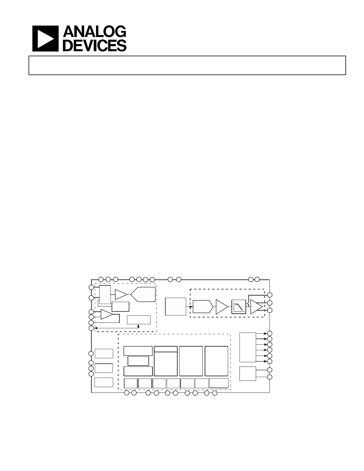
Figure 1. Basic Block Diagram
Rev. PrA
Information furnished by Analog Devices is believed to be accurate and reliable.
However, no responsibility is assumed by Analog Devices for its use, nor for any
infringements of patents or other rights of third parties that may result from its use.
Specifications subject to change without notice. No license is granted by implication
or otherwise under any patent or patent rights of Analog Devices. Trademarks and
registered trademarks are the property of their respective companies.
One Technology Way, P.O. Box 9106, Norwood, MA 02062-9106, U.S.A.
Tel: 781.329.4700
www.analog.com
HT TH
Fax: 781.326.8703 © 2006 Analog Devices, Inc. All rights reserved.
1 page 
Preliminary Technical Data
Parameter
Flash/EE MEMORY7,8
Endurance
Data Retention
Digital Inputs
Logic 1 Input Current
(leakage Current )
Logic 0 Input Current
(leakage Current )
Input Capacitance
Logic Inputs3
VINL, Input Low Voltage
VINH, Input High Voltage
Quadrature Encoder Inputs S1/S2/CLR
(Schmitt-Triggered Inputs)
VBT+
VBT-
V -VT+ T-B B
BB
Logic Outputs9
VOH, Output High Voltage
VOL, Output Low Voltage
CRYSTAL INPUTS XCLKI and XCLKO
Logic Inputs, XCLKI Only
VINL, Input Low Voltage
VINH, Input High Voltage
XCLKI Input Capacitance
XCLKO Output Capacitance
MCU CLOCK RATE (PLL)
INTERNAL OSCILLATOR
Tolerance
STARTUP TIME
At Power-On
From Pause/Nap Mode
From Sleep Mode
From Stop Mode
Programmable Logic Array (PLA)
Pin Propagation Delay
ADuC7128
10,000
20
±1
±0.2
-60
-40
-120
-80
10
0.8
2.0
1.9
2.1
0.9
1.1
0.9
1.1
IOVDDB B – 400mV
0.4
1.1
1.7
20
20
326.4
41.779200
32.768
±3
TBD
TBD
TBD
TBD
12
ADuC7128
Unit
Cycles min
Years min
µA max
µA typ
µA max
µA typ
µA max
µA typ
pF typ
V max
V min
Test Conditions/Comments
TJB B = 85°C
All digital inputs including XCLKI and XCLKO
VINH = VDD or VINH = 5V
VINL = 0V, except TDI
VINL = 0V, TDI Only
All Logic inputs including XCLKI and XCLKO
V min
V max
V min
V max
V min
V max
V min
V max
IBSOURCEB = 1.6mA
IBSINKB = 1.6mA
V
V
pF
pF
kHz min
MHz max
kHz typ
% max
8 programmable core clock selections within this
range.
(32.768kHz x 1275)/128
(32.768kHz x 1275)/1
Core Clock = 41.78 MHz
ns typ
From input pin to output pin
Rev. PrA | Page 5 of 92
5 Page 
Preliminary Technical Data
ADuC7128
Table 5. SPI Slave Mode Timing (PHASE Mode = 1)
Parameter
Description
tCSB B
CS to SCLOCK edge1
TP PT
tSLB B
SCLOCK low pulsewidth2
TP PT
tSHB B SCLOCK high pulsewidth2
tBDAVB Data output valid after SCLOCK edge
Min
2 × tBUCLKB
Typ
(SPIDIV + 1) × tBHCLKB
(SPIDIV + 1) × tBHCLKB
tBDSUB Data input setup time before SCLOCK edge1
tBDHDB Data input hold time after SCLOCK edge1
tDFB B Data output fall time
tDRB B Data output rise time
tSRB B SCLOCK rise time
tSFB B SCLOCK fall time
tBSFSB CS high after SCLOCK edge
1 × tBUCLKB
2 × tBUCLKB
0
1
TP PT
tBUCLKB
=
23.9
ns.
It
corresponds
to
the
41.78
MHz
internal
clock
from
the
PLL
before
the
clock
divider.
2
TP PT
tBHCLKB
depends
on
the
clock
divider
or
CD
bits
in
PLLCON
MMR.
TBHCLKB
=
t /2 .BUCLKB
CD
PP
5
5
5
5
Max
2x
t +BHCLK
2×
tBUCLKB
12.5
12.5
12.5
12.5
Unit
ns
ns
ns
ns
ns
ns
ns
ns
ns
ns
ns
CS
SCLOCK
(POLARITY = 0)
SCLOCK
(POLARITY = 1)
MISO
MOSI
tCS
tSH
tDAV
tSL
tDF
MSB
tSR
tDR
BITS 6–1
tDSU
MSB IN
tDHD
BITS 6–1
Figure 6. SPI Slave Mode Timing (PHASE Mode = 1)
tSFS
tSF
LSB
LSB IN
Rev. PrA | Page 11 of 92
11 Page | ||
| Páginas | Total 30 Páginas | |
| PDF Descargar | [ Datasheet ADUC7128.PDF ] | |
Hoja de datos destacado
| Número de pieza | Descripción | Fabricantes |
| ADuC7121 | Precision Analog Microcontroller 12-Bit Analog I/O ARM7TDMI MCU | Analog Devices |
| ADUC7122 | Precision Analog Microcontroller | Analog Devices |
| ADUC7124 | ARM7TDMI MCU | Analog Devices |
| ADUC7126 | ARM7TDMI MCU | Analog Devices |
| Número de pieza | Descripción | Fabricantes |
| SLA6805M | High Voltage 3 phase Motor Driver IC. |
Sanken |
| SDC1742 | 12- and 14-Bit Hybrid Synchro / Resolver-to-Digital Converters. |
Analog Devices |
|
DataSheet.es es una pagina web que funciona como un repositorio de manuales o hoja de datos de muchos de los productos más populares, |
| DataSheet.es | 2020 | Privacy Policy | Contacto | Buscar |