|
|
|
PDF DS3100DK Data sheet ( Hoja de datos )
| Número de pieza | DS3100DK | |
| Descripción | Stratum 3/E3 Timing Card IC Demo KIT | |
| Fabricantes | Maxim Integrated Products | |
| Logotipo | ||
Hay una vista previa y un enlace de descarga de DS3100DK (archivo pdf) en la parte inferior de esta página. Total 30 Páginas | ||
|
No Preview Available !
www.DataSheet4U.com
www.maxim-ic.com
GENERAL DESCRIPTION
The DS3100DK is an easy-to-use demo and
evaluation kit for the DS3100 Stratum 3/3E timing
card IC. A surface-mounted DS3100 and careful
layout provide maximum signal integrity. An on-board
Dallas 8051-compatible microcontroller and included
software give point-and-click access to configuration
and status registers from a personal computer. LEDs
on the board indicate interrupt, power-supply
function, and GPIO status. The board provides BNC
and bantam connectors for the composite clock and
BITS interfaces. Single-ended and LVDS clocks are
accessed via SMB connectors. All LEDs and
connectors are clearly labeled with silkscreening to
identify associated signals.
DEMO KIT CONTENTS
DS3100DK PCB
CD_ROM Includes:
DS3100 Software
DS3100 Initialization files
DS3100DK Data Sheet
DS3100 Data Sheet/Errata Sheet
DS3100DK
Stratum 3/E3 Timing Card IC
Demo Kit
FEATURES
Soldered DS3100 for Best Signal Integrity
SMB Connectors, BNC, Bantam,
Transformers, and Termination Ease
Connectivity
Careful Layout for Analog Signal Paths
On-Board Stratum 3 Oscillator with Footprints
for Stratum 3E Oscillators
DS3100 Configured for CPU Bus Operation
for Complete Control Over the Device
On-Board Dallas Microcontroller and Included
Software Provide Point-and-Click Access to
the DS3100 Register Set
LEDs for Interrupt, Power Supplies, and GPIO
Included International Power Supply
Banana Jack VDD and GND Connectors
Support Use of Lab Power Supplies
Easy-to-Read Silkscreen Labels Identify the
Signals Associated with All Connectors,
Jumpers and LEDs
Header Provided for Master/Slave Connection
to a Second DS3100DK
MINIMUM SYSTEM REQUIREMENTS
PC Running Windows® XP or Windows 2000
Display with 1024 x 768 Resolution or Higher
Available Serial (COM) Port
DB-9 Serial Cable
ORDERING INFORMATION
PART
DS3100DK
DESCRIPTION
Demo kit for DS3100
Windows is a registered trademark of Microsoft Corp.
DataSheet4 U .com
1 of 32
REV: 091806
1 page 
www.DataSheet4U.com
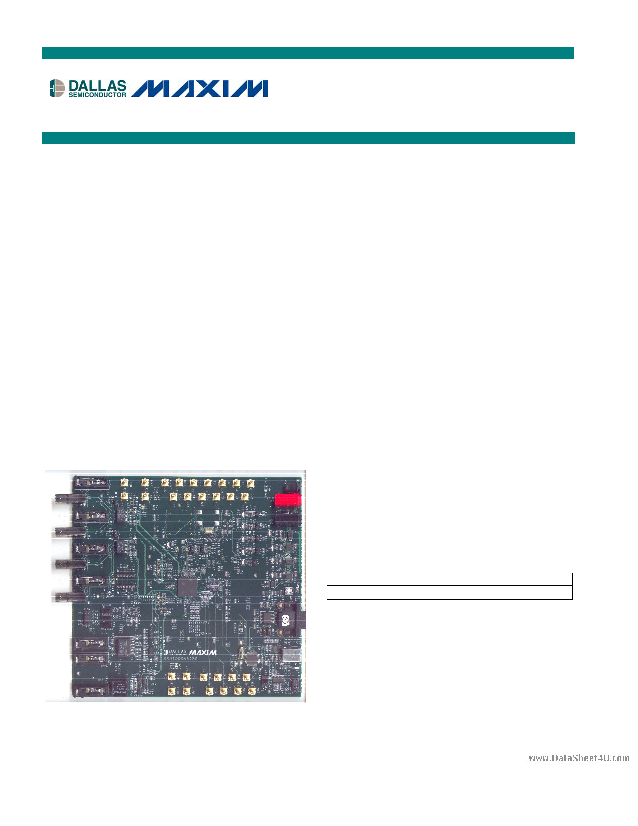
DS3100DK
1.1 Input and Output Clocks
There are 13 SMB connectors at the top of the board labeled IC1–IC4, IC7–IC14, and SYNC2K that provide a
single-ended clock input to the DS3100. All single-ended clock inputs are connected to the DS3100 with a 50Ω
characteristic impedance trace and terminated with 50Ω at the device. Four additional SMB connectors labeled
IC5P, IC5N, IC6P, and IC6N provide differential clock inputs to the DS3100. These differential inputs have 50Ω
trace impedance and 50Ω termination at the device (i.e., 100Ω differential).
On the other end of the PCB are eight SMB clock output connectors labeled OC1–OC5 and OC9, OC10, and
OC11. All single-ended clock outputs are buffered at the DS3100 and connected to the SMB connector via a 50Ω
characteristic impedance trace. Four additional SMB connectors labeled OC6P, OC6N, OC7P, and OC7N provide
connections to the differential outputs from the DS3100.
1.2 Jumpers, Headers, and Switch Settings
Jumpers JMP1 to JMP4 (upper right of board) provide input settings to the four DS3100 GPIO pins. If a jumper is
installed the corresponding GPIO input is high. With no jumper the GPIO pin defaults low. LEDs DS5–DS8 indicate
the logic level of the GPIO pins (LED lit means GPIO pin is high). Switches SW7 to SW9 set the SONSDH,
SRCSW and MASTSLV pins, respectively, high or low as indicated by the silkscreen. Headers J1 and J2 provide
access to BITS1 and BITS2 framer signals, respectively. Header J51 provides access to the JTAG port of the
DS3100. Header J15 provides interface to a master or slave board depending on position of switch SW6.
1.3 Composite Clock Interface
Bantam jacks J89 and J90 provide access to composite clock inputs IC1A and IC2A through a 2:1 transformer.
Jumpers JMP7 and JMP6 configure termination for IC1A and IC2A respectively. Silkscreen text indicates which
jumper is necessary to set the interface at 110Ω, 120Ω, or 133Ω. Bantam jack J117 provides an interface through a
1:1 transformer to the OC8 composite clock output. Jumpers JMP8, JMP9, and JMP10 provide different attenuation
configurations that are represented in silkscreen (Rs = 91Ω with no jumper installed). See the schematics for
additional details on the composite clock termination circuitry.
1.4 BITS Interfaces
The BITS1 DS1/E1 LIU uses bantam connectors J85 and J55 or BNC connectors J83 and J57 for transmit and
receive interfaces, respectively. The BITS2 LIU uses bantam connectors J86 and J56 or BNC connectors J84 and
J58 for transmit and receive, respectively. There is a dual transformer package for each BITS transceiver
(component T1 for BITS1 and T2 for BITS2). See the schematics for additional details on the BITS termination
circuitry.
1.5 Microcontroller
The DS87C520 microcontroller has factory-installed firmware in on-chip nonvolatile memory. This firmware
translates memory access requests from the RS-232 serial port or USB port into register accesses on the DS3100.
When the microcontroller starts up it turns on DS16 to indicate that the controller is working correctly. A pushbutton
switch labeled RESET (SW5) at the right middle of the board resets the microcontroller as well as the DS3100.
1.6 Power-Supply Connectors
The included international power supply can be connected to jack J3 to power the board or a 5V lab power supply
can be connected across the red (J13) and black (J19) banana jacks. The 5V input is then regulated to 3.3V and
1.8V and distributed to board components.
DataSheet4 U .com
5 of 32
5 Page 
www.DataSheet4U.com
DS3100DK
4.7 Output Clocks
The fields in this box configure the DS3100’s 11 output clocks. The 2K8K field specifies the source (T0 path or T4
path) for the 2kHz and 8kHz clock options for output clocks OC1–OC7. Similarly the DIG1 and DIG2 fields
configure the Digital1 and Digital2 frequency options for OC1–OC7 (see the DS3100 data sheet for details).
The OC1–OC7 fields specify the output frequencies for outputs OC1–OC7. Note that when the T0 APLL setting is
changed, the frequencies of all the T0 options in the OC1–OC7 fields automatically change to frequencies derived
from the new T0 APLL frequency. Similarly, when the T4 APLL setting is changed, the frequencies of all the T4
options in the OC1–OC7 fields automatically change to frequencies derived from the new T4 APLL frequency.
These changes match what happens inside the DS3100 device.
The OC89 field specifies whether the T0 path or the T4 path is the source for output clocks OC8 and OC9. OC8 is
the 64kHz composite clock output. The OC8 field configures the OC8 output clock for 50% or 5/8 duty cycle, and
also for whether or not the output signal has 8kHz BPVs and optionally 400Hz absence-of-BPVs per ITU-T G.703
Appendix II options a) and b). The “8K” options in the list enable the 8kHz BPVs but not the 400Hz absence-of-
BPVs. The “400” options enable both the 8kHz BPVs and the 400Hz absence-of-BPVs. OC9 is a dedicated
1.544MHz or 2.048MHz output. When OC89 specifies that OC8 and OC9 are sourced from the T4 path, the Auto
Squelch checkbox specifies whether or not OC8 and OC9 are automatically squelched when T4 has no valid input
references. When OC89 indicates T0 path, Auto Squelch is not available to match DS3100 behavior.
OC10 is an 8kHz output that can be configured as a 50% duty cycle clock or a frame pulse and can optionally be
inverted. OC11 is a 2kHz output that can be similarly configured.
Table 4-6. Mapping Between Software Fields and DS3100 Register Fields
SOFTWARE FIELD
2K8K
DIG1
DIG2
OC1–OC7
OC89
Auto Squelch
OC8
OC9
OC10
OC11
DS3100 REGISTER FIELDS
FSCR1:2K8KSRC
MCR6:DIG1SS, MCR7:DIG1F
MCR6:DIG2SS, MCR7:DIG2F, MCR7:DIG2AF
OCR1–OCR4
MCR4:OC89
T4CR1:ASQUEL
OCR4:OC8EN, T4CR1:OC8DUTY MCR8:OC8NO8,
MCR8:OC8400
OCR4:OC9EN, T4CR1:OC9SON
OCR4:OC10EN, FSCR1:8KPUL, FSCR1:8KINV
OCR4:OC11EN, FSCR1:2KPUL, FSCR1:2KINV
DataSheet4 U .com
11 of 32
11 Page | ||
| Páginas | Total 30 Páginas | |
| PDF Descargar | [ Datasheet DS3100DK.PDF ] | |
Hoja de datos destacado
| Número de pieza | Descripción | Fabricantes |
| DS3100DK | Stratum 3/E3 Timing Card IC Demo KIT | Maxim Integrated Products |
| Número de pieza | Descripción | Fabricantes |
| SLA6805M | High Voltage 3 phase Motor Driver IC. |
Sanken |
| SDC1742 | 12- and 14-Bit Hybrid Synchro / Resolver-to-Digital Converters. |
Analog Devices |
|
DataSheet.es es una pagina web que funciona como un repositorio de manuales o hoja de datos de muchos de los productos más populares, |
| DataSheet.es | 2020 | Privacy Policy | Contacto | Buscar |