|
|
|
PDF ADT7470 Data sheet ( Hoja de datos )
| Número de pieza | ADT7470 | |
| Descripción | Temperature Sensor Hub and Fan Controller | |
| Fabricantes | Analog Devices | |
| Logotipo | ||
Hay una vista previa y un enlace de descarga de ADT7470 (archivo pdf) en la parte inferior de esta página. Total 30 Páginas | ||
|
No Preview Available !
Data Sheet
Temperature Sensor Hub and Fan Controller
ADT7470
FEATURES
Monitors up to 10 remote temperature sensors
Monitors and controls speed of up to 4 fans independently
PWM outputs drive each fan under software control
FULL_SPEED input allows fans to be blasted to maximum
speed by external hardware
SMBALERT interrupt signals failures to system controller
Three-state ADDR pin allows up to 3 devices on a single bus
Temperature decoder interprets TMP05 temperature sensors
and communicates values over I2C bus
Limit comparison of all monitored values
Supports fast I2C standard (400 kHz max)
Meets SMBus 2.0 electrical specifications
(fully SMBus 1.1-compliant)
APPLICATIONS
Servers
Networking and telecommunications equipment
Desktops
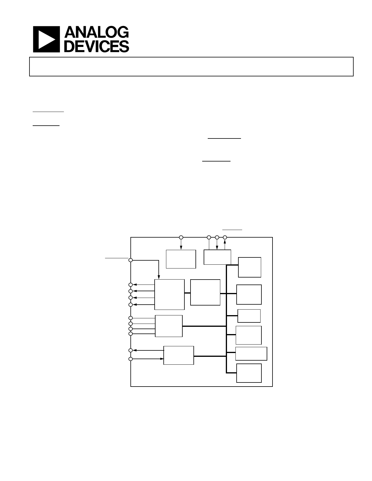
GENERAL DESCRIPTION
The ADT74701 controller is a multichannel temperature sensor
and PWM fan controller and fan speed monitor for systems
requiring active cooling. It is designed to interface directly to
an I2C® bus. The ADT7470 can monitor up to 10 daisy-chained
TMP05 temperature sensors. It can also monitor and control
the speed of four fans, in automatic or in manual control loops.
A FULL_SPEED input is provided to allow the fans to be
blasted to maximum speed, via external hardware control,
under extreme thermal conditions or on system startup. An
SMBALERT interrupt communicates error conditions such as
fan under speed and over temperature measurements to the
system service processor. Individual error conditions can then
be read from status registers over the I2C bus.
FUNCTIONAL BLOCK DIAGRAM
ADDR
SDA SCL SMBALERT
ADT7470
FULL_SPEED
SMBus
ADDRESS
SELECTION
SERIAL BUS
INTERFACE
ADDRESS
POINTER
REGISTER
PWM1
PWM2
PWM3
PWM4
TACH1
TACH2
TACH3
TACH4
TMP_START
TMP_IN
PWM
REGISTERS
AND
CONTROLLERS
AUTOMATIC
FAN SPEED
CONTROL
FAN SPEED
COUNTERS
TEMPERATURE
DECODER
Figure 1.
PWM
CONFIG
REGISTERS
INTERRUPT
MASKING
INTERRUPT
STATUS
REGISTERS
LIMIT
COMPARATORS
VALUE AND
LIMIT
REGISTERS
1 Protected by Patent Numbers US6,169,442, US6,097,239, US5,982,221, US5,867,012. Other patents pending.
Rev. E
Document Feedback
Information furnished by Analog Devices is believed to be accurate and reliable. However, no
responsibilityisassumedbyAnalogDevices for itsuse,nor foranyinfringementsofpatentsor other
rights of third parties that may result from its use. Specifications subject to change without notice. No
license is granted by implication or otherwise under any patent or patent rights of Analog Devices.
Trademarksandregisteredtrademarksarethepropertyoftheirrespectiveowners.
One Technology Way, P.O. Box 9106, Norwood, MA 02062-9106, U.S.A.
Tel: 781.329.4700 ©2004–2013 Analog Devices, Inc. All rights reserved.
Technical Support
www.analog.com
1 page 
ADT7470
Data Sheet
SERIAL BUS TIMING SPECIFICATIONS
Table 2.
Parameter1, 2, 3, 4, 5
SERIAL BUS TIMING
Clock Frequency, fSCLK
Glitch Immunity, tSW
Bus Free Time, tBUF
Start Setup Time, tSU;STA
Start Hold Time, tHD;STA
SCL Low Time, tLOW
SCL High Time, tHIGH
SCL, SDA Rise Time, tr
SCL, SDA Fall Time, tf
Data Setup Time, tSU;DAT
Detect Clock Low Timeout, tTIMEOUT
Min Typ Max Unit
50
1.3
600
600
1.3
0.6
100
25 28
400 kHz
ns
μs
ns
ns
μs
μs
300 ns
300 ns
ns
31 ms
Test Conditions/Comments
See Figure 2
See Figure 2
See Figure 2
See Figure 2
See Figure 2
See Figure 2
See Figure 2
See Figure 2
See Figure 2
See Figure 2
Can be optionally disabled,
via Configuration Register 1
(see Table 6)
1 VDD should never be floated in the presence of SCL/SDA activity. Charge injection can be sufficient to induce approximately 0.6 V on VDD.
2 All voltages are measured with respect to GND, unless otherwise specified.
3 Typical values are at %A = 25°C and represent the most likely parametric norm.
4 Logic inputs accept input high voltages up to 5 V even when the device is operating at supply voltages below 5 V.
5 Timing specifications are tested at logic levels of VIL = 0.8 V for a falling edge and VIH = 2.0 V for a rising edge.
SCL
tLOW
tR
tHD;STA
tHD;DAT
SDA
tBUF
PS
tF
tHIGH
tSU;DAT
tHD;STA
tSU;STA
S
Figure 2. Serial Bus Timing Diagram
tSU;STO
P
Rev. E | Page 4 of 40
5 Page 
ADT7470
Data Sheet
during the low period before the 10th clock pulse, then
high during the 10th clock pulse to assert a stop condition.
Any number of bytes of data can be transferred over the serial
bus in one operation. However, it is not possible to mix read
and write in one operation, because the type of operation is
determined at the beginning and subsequently cannot be
changed without starting a new operation.
In the ADT7470, write operations contain either one or two
bytes, and read operations contain one byte and perform the
following functions.
1
SCL
9
To write data to one of the device data registers or read data
from it, the address pointer register must be set so that the
correct data register is addressed. Then data can be written into
that register or read from it. The first byte of a write operation
always contains an address that is stored in the address pointer
register. If data is to be written to the device, the write operation
contains a second data byte that is written to the register selected
by the address pointer register.
This is illustrated in Figure 7. The device address is sent over the
bus followed by R/W set to 0. This is followed by two data bytes.
19
SDA
START BY
MASTER
0
1
01
1 A1 A0 R/W
D7
FRAME 1
SERIAL BUS ADDRESS
BYTE
ACK. BY
ADT7470
1
SCL (CONTINUED)
D6 D5 D4 D3 D2 D1 D0
FRAME 2
ADDRESS POINTER REGISTER BYTE
ACK. BY
ADT7470
9
SDA (CONTINUED)
D7 D6 D5 D4 D3 D2 D1 D0
FRAME 3
DATA
BYTE
ACK. BY STOP BY
ADT7470 MASTER
Figure 7. Writing a Register Address to the Address Pointer Register, Then Writing Data to the Selected Register
SCL
1
91
9
SDA
START BY
MASTER
0
1
01
1 A1 A0 R/W
D7 D6 D5 D4 D3 D2 D1 D0
FRAME 1
SERIAL BUS ADDRESS
BYTE
ACK. BY
ADT7470
FRAME 2
ADDRESS POINTER REGISTER BYTE
Figure 8. Writing to the Address Pointer Register Only
ACK. BY STOP BY
ADT7470 MASTER
SCL
1
91
9
SDA
START BY
MASTER
0
1
01
1 A1 A0 R/W
D7 D6 D5 D4 D3 D2
FRAME 1
SERIAL BUS ADDRESS
BYTE
ACK. BY
ADT7470
FRAME 2
DATA BYTE FROM
ADT7470
Figure 9. Reading Data from a Previously Selected Register
D1
D0
NO ACK. STOP BY
BY MASTER MASTER
Rev. E | Page 10 of 40
11 Page | ||
| Páginas | Total 30 Páginas | |
| PDF Descargar | [ Datasheet ADT7470.PDF ] | |
Hoja de datos destacado
| Número de pieza | Descripción | Fabricantes |
| ADT7470 | Temperature Sensor Hub and Fan Controller | Analog Devices |
| ADT7473 | Remote Thermal Monitor and Fan Control | ON Semiconductor |
| ADT7473 | dBCool Remote Thermal Monitor and Fan Controller | Analog Devices |
| ADT7475 | Remote Thermal Monitor and Fan Controller | ON Semiconductor |
| Número de pieza | Descripción | Fabricantes |
| SLA6805M | High Voltage 3 phase Motor Driver IC. |
Sanken |
| SDC1742 | 12- and 14-Bit Hybrid Synchro / Resolver-to-Digital Converters. |
Analog Devices |
|
DataSheet.es es una pagina web que funciona como un repositorio de manuales o hoja de datos de muchos de los productos más populares, |
| DataSheet.es | 2020 | Privacy Policy | Contacto | Buscar |