|
|
PDF ADG3301 Data sheet ( Hoja de datos )
| Número de pieza | ADG3301 | |
| Descripción | Single-Channel Bidirectional Logic Level Translator | |
| Fabricantes | Analog Devices | |
| Logotipo |  |
|
Hay una vista previa y un enlace de descarga de ADG3301 (archivo pdf) en la parte inferior de esta página. Total 20 Páginas | ||
|
No Preview Available !
www.DataSheet4U.com
Low Voltage 1.15 V to 5.5 V, Single-Channel
Bidirectional Logic Level Translator
ADG3301
FEATURES
Bidirectional level translation
Operates from 1.15 V to 5.5 V
Low quiescent current < 5 µA
No direction pin
APPLICATIONS
SPI®, MICROWIRE® level translation
Low voltage ASIC level translation
Smart card readers
Cell phones and cell phone cradles
Portable communication devices
Telecommunications equipment
Network switches and routers
Storage systems (SAN/NAS)
Computing/server applications
GPS
Portable POS systems
Low cost serial interfaces
GENERAL DESCRIPTION
The ADG3301 is a single-channel, bidirectional logic level
translator. It can be used in multivoltage digital system applica-
tions such as data transfer between a low voltage DSP/controller
and a higher voltage device. The internal architecture allows the
device to perform bidirectional logic level translation without an
additional signal to set the direction in which the translation
takes place.
The voltage applied to VCCA sets the logic levels on the A side of
the device, while VCCY sets the levels on the Y side. For proper
operation, VCCA must always be less than VCCY. The VCCA-
compatible logic signals applied to the A pin appear as VCCY-
compatible levels on the Y pin. Similarly, VCCY-compatible logic
levels applied to the Y pin appear as VCCA-compatible logic levels
on the A pin. The enable pin (EN) provides three-state operation
on both the A pin and the Y pin. When the device enable pin is
pulled low, the terminals on both sides of the device are in the
high impedance state. The EN pin is referred to the VCCA supply
voltage and driven high for normal operation.
The ADG3301 is available in a compact 6-lead SC70 package
and is guaranteed to operate over the 1.15 V to 5.5 V supply
voltage range and extended −40°C to +85°C temperature range.
FUNCTIONAL BLOCK DIAGRAM
VCCA
VCCY
AY
EN ADG3301
GND
Figure 1.
PRODUCT HIGHLIGHTS
1. Bidirectional level translation.
2. Fully guaranteed over the 1.15 V to 5.5 V supply range.
3. No direction pin.
4. Compact 6-lead SC70 package.
Rev. 0
Information furnished by Analog Devices is believed to be accurate and reliable. However, no
responsibility is assumed by Analog Devices for its use, nor for any infringements of patents or other
rights of third parties that may result from its use. Specifications subject to change without notice. No
license is granted by implication or otherwise under any patent or patent rights of Analog Devices.
Trademarksandregisteredtrademarksarethepropertyoftheirrespectiveowners.
One Technology Way, P.O. Box 9106, Norwood, MA 02062-9106, U.S.A.
Tel: 781.329.4700
www.analog.com
Fax: 781.461.3113
© 2005 Analog Devices, Inc. All rights reserved.
1 page 
Parameter1
POWER REQUIREMENTS
Power Supply Voltages
Quiescent Power Supply Current
Symbol
VCCA
VCCY
ICCA
ICCY
Three-State Mode Power Supply Current
IHiZA
IHiZY
1 Temperature range for the B version is −40°C to +85°C.
2 All typical values are at TA = 25°C, unless otherwise noted.
3 Guaranteed by design, not subject to production test.
Conditions
VCCA ≤ VCCY
VA = 0 V/VCCA, VY = 0 V/VCCY,
VCCA = VCCY = 5.5 V, EN = 1
VA = 0 V/VCCA, VY = 0 V/VCCY,
VCCA = VCCY = 5.5 V, EN = 1
VCCA = VCCY = 5.5 V, EN = 0
VCCA = VCCY = 5.5 V, EN = 0
ADG3301
Min Typ2 Max Unit
1.15 5.5
1.65 5.5
0.17 5
0.27 5
0.1 5
0.1 5
V
V
µA
µA
µA
µA
Rev. 0 | Page 5 of 20
5 Page 
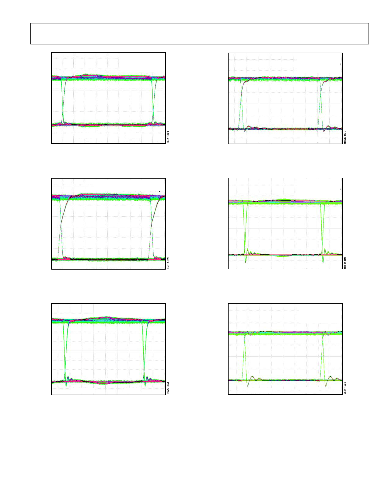
TA = 25°C
DATA RATE = 25Mbps
CL = 50pF
1 CHANNEL
400mV/DIV
5ns/DIV
Figure 21. Eye Diagram at Y Output
(1.2 V to 1.8 V Level Translation, 25 Mbps)
TA = 25°C
CL = 15pF
DATA RATE = 25Mbps 1 CHANNEL
ADG3301
TA = 25°C
DATA RATE = 50Mbps
CL = 15pF
1 CHANNEL
400mV/DIV
3ns/DIV
Figure 24. Eye Diagram at A Output
(3.3 V to 1.8 V Level Translation, 50 Mbps)
TA = 25°C
DATA RATE = 50Mbps
CL = 50pF
1 CHANNEL
200mV/DIV
5ns/DIV
Figure 22. Eye Diagram at A Output
(1.8 V to 1.2 V Level Translation, 25 Mbps)
TA = 25°C
CL = 50pF
DATA RATE = 50Mbps 1 CHANNEL
1V/DIV
3ns/DIV
Figure 25. Eye Diagram at Y Output
(3.3 V to 5 V Level Translation, 50 Mbps)
TA = 25°C
DATA RATE = 50Mbps
CL = 15pF
1 CHANNEL
500mV/DIV
3ns/DIV
Figure 23. Eye Diagram at Y Output
(1.8 V to 3.3 V Level Translation, 50 Mbps)
800mV/DIV
3ns/DIV
Figure 26. Eye Diagram at A Output
(5 V to 3.3 V Level Translation, 50 Mbps)
Rev. 0 | Page 11 of 20
11 Page | ||
| Páginas | Total 20 Páginas | |
| PDF Descargar | [ Datasheet ADG3301.PDF ] | |
Hoja de datos destacado
| Número de pieza | Descripción | Fabricantes |
| ADG3300 | 8-Channel Bidirectional Logic Level Translator | Analog Devices |
| ADG3301 | Single-Channel Bidirectional Logic Level Translator | Analog Devices |
| ADG3304 | Bidirectional Logic Level Translator | Analog Devices |
| ADG3308 | 8-Channel Bidirectional Logic Level Translators | Analog Devices |
| Número de pieza | Descripción | Fabricantes |
| SLA6805M | High Voltage 3 phase Motor Driver IC. |
Sanken |
| SDC1742 | 12- and 14-Bit Hybrid Synchro / Resolver-to-Digital Converters. |
Analog Devices |
|
DataSheet.es es una pagina web que funciona como un repositorio de manuales o hoja de datos de muchos de los productos más populares, |
| DataSheet.es | 2020 | Privacy Policy | Contacto | Buscar |
