|
|
|
PDF AD8311 Data sheet ( Hoja de datos )
| Número de pieza | AD8311 | |
| Descripción | 50 dB GSM PA Controller | |
| Fabricantes | Analog Devices | |
| Logotipo | ||
Hay una vista previa y un enlace de descarga de AD8311 (archivo pdf) en la parte inferior de esta página. Total 25 Páginas | ||
|
No Preview Available !
FEATURES
Complete RF detector/controller function
>50 dB range at 0.9 GHz (−48 dBm to +3 dBm re 50 Ω)
Accurate scaling from 0.1 GHz to 2.5 GHz
Temperature-stable linear-in-dB response
Log slope of 23 mV/dB, intercept at −60 dBm at 0.9 GHz
True integration function in control loop
Low power: 20 mW at 2.7 V
APPLICATIONS
Single, dual, and triple band mobile handset (GSM, DCS,
EDGE)
Transmitter power control
GENERAL DESCRIPTION
The AD8311 is a complete low cost subsystem for the precise
control of RF power amplifiers operating in the frequency range
0.1 GHz to 2.5 GHz and over a typical dynamic range of 50 dB.
It is intended for use in cellular handsets and other battery-
operated wireless devices. The log amp technique provides a
much wider measurement range and better accuracy than
controllers using diode detectors. In particular, its temperature
stability is excellent over a specified range of −40°C to +85°C.
50 dB GSM PA Controller
AD8311
Its high sensitivity allows control at low signal levels, thus
reducing the amount of power that needs to be coupled to the
detector. For convenience, the signal is internally ac-coupled.
This high-pass coupling, with a corner at approximately
0.016 GHz, determines the lowest operating frequency. Thus,
the source can be dc-grounded.
The AD8311 provides a voltage output, VAPC, which has the
voltage range and current drive to directly connect to the gain
control pin of most handset power amplifiers. VAPC can swing
from 300 mV above ground to within 200 mV below the supply
voltage. Load currents of up to 6 mA can be supported.
The setpoint control input is applied to pin VSET and has an
operating range of 0.25 V to 1.4 V. The associated circuit
determines the slope and intercept of the linear-in-dB
measurement system; these are nominally 23.6 mV/dB and
−59.7 dBm at 0.9 GHz. Further simplifying the application of
the AD8311, the input resistance of the setpoint interface is over
35 MΩ, and the bias current is typically 0.26 μA.
The AD8311 is available in a 6-ball wafer-level chip scale
package (WLCSP), 1.0 mm × 1.5 mm, and consumes 7.6 mA
from a 2.7 V to 5.5 V supply.
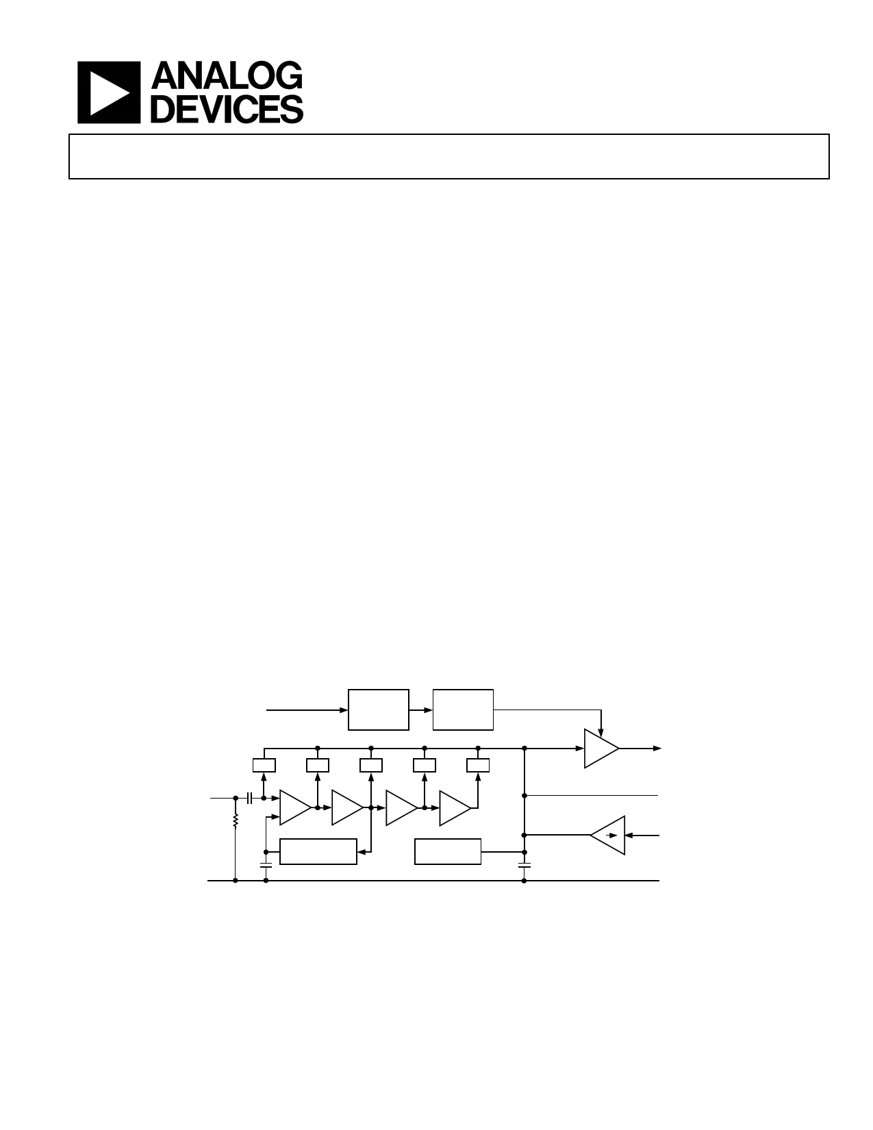
FUNCTIONAL BLOCK DIAGRAM
VPOS
LOW NOISE
GAIN BIAS
LOW NOISE
BAND GAP
REFERENCE
RFIN
DET
DET
DET
DET
DET
10dB
10dB
10dB
10dB
COMM
OFFSET
COMPENSATION
INTERCEPT
POSITIONING
Figure 1.
⋅ 1.35
VAPC
HI-Z
LOW NOISE
RAIL-TO-RAIL BUFFER
FLTR
VSET
VI
23mV/dB
250mV TO
1.4V = 50dB
Rev. A
Information furnished by Analog Devices is believed to be accurate and reliable. However, no
responsibility is assumed by Analog Devices for its use, nor for any infringements of patents or other
rights of third parties that may result from its use. Specifications subject to change without notice. No
license is granted by implication or otherwise under any patent or patent rights of Analog Devices.
Trademarksandregisteredtrademarksarethepropertyoftheirrespectiveowners.
One Technology Way, P.O. Box 9106, Norwood, MA 02062-9106, U.S.A.
Tel: 781.329.4700
www.analog.com
Fax: 781.461.3113 ©2005–2011 Analog Devices, Inc. All rights reserved.
1 page 
AD8311
Parameter
Conditions
MEASUREMENT MODE (f = 2.5 GHz)
Input Impedance
No termination resistor on RFIN
±1 dB Dynamic Range
TA = +25°C
Maximum Input Level
−40°C < TA < +85°C
±1 dB error
Minimum Input Level
Slope2
Intercept2
±1 dB error
VSET Voltage—High Power In
VSET Voltage—Low Power In
Temperature Sensitivity
PIN = –10 dBm
PIN = –40 dBm
PIN = –10 dBm
25°C ≤ TA ≤ 85°C
OUTPUT INTERFACE
−40°C ≤ TA ≤ +25°C
VAPC (Pin 2)
Minimum Output Voltage
Maximum Output Voltage
vs. Temperature
General Limit
Output Current Drive
Output Noise
Small Signal Bandwidth
VSET ≤ 150mV
IOUT = 3 mA
RL = ∞
85°C, VPOS = 3 V, IOUT = 6 mA
2.7 V ≤ VPOS ≤ 5.5 V, RL = ∞
VSET = 1.5 V, RFIN = –50 dBm, source/sink
RF Input = 2 GHz, 0 dBm, fNOISE = 100 kHz, CFLT = 220 pF
RFIN = −10 dBm; from FLTR to VAPC
Fall Time
Input level = off to 0 dBm, 90% to 10%
Rise Time
Input level = 0 dBm to off, 10% to 90%
Slew Rate
Response Time
90% – 10%, VSET = 0.3 V, open loop
FLTR = Open
VSET INTERFACE
VSET (Pin 3)
Nominal Input Range
RFIN = 0 dBm; measurement mode
RFIN = −50 dBm; measurement mode
Logarithmic Scale Factor
Bias Current Source
RFIN = −10 dBm; VSET = 1.4 V
Input Resistance
Slew Rate
POWER INTERFACE
VPOS (Pin 1)
Supply Voltage
Quiescent Current
vs. Temperature
Power-On Time
Power-Off Time
–40°C ≤ TA ≤ +85°C
Time from VPOS high to VAPC within 1% of final value,
VSET ≤ 200 mV
Time from VPOS low to VAPC within 1% of final value,
VSET ≤ 200 mV
1 VAPC (Pin 2) to VSET (Pin 3) with inversion stage, sinusoidal input signal.
2 Mean and standard deviation specifications are available in Table 4.
Min Typ
Max Unit
164 || 1.55
42
41
−6.2
−47.7
22.5
−60.6
1.14
0.46
Ω || pF
dB
dB
dBm
dBm
mV/dB
dBm
V
V
−0.0004
+0.0090
dB/°C
dB/°C
0.2 0.3
0.4 V
2.3 2.55 V
2.4 2.65 V
2.54 V
VPOS – 0.1
V
5/200
mA/μA
170 nV/√Hz
30 MHz
120 ns
270 ns
15 V/μs
130 ns
1.4 V
0.27 V
0.04 dB/mV
0.26 μA
36 MΩ
14 V/μs
2.7
5 7.6
8.2
3
100
5.5 V
10.7 mA
12.9 mA
10 μs
2000 ns
Rev. A | Page 4 of 24
5 Page 
AD8311
25
23
–40°C
+25°C
23
22
+85°C
21
0 0.5 1.0 1.5 2.0 2.5
FREQUENCY (GHz)
Figure 21. Slope vs. Frequency
−40°C, +25°C, and +85°C
25
23
0.1GHz
0.9GHz
23
1.9GHz
2.5GHz
22
21
2.5
3.0 3.5 4.0 4.5 5.0
VPOS (V)
Figure 22. Slope vs. Supply Voltage
5.5
–55
–57
–59
+25°C
–61
–40°C
+85°C
–63
–65
0
–58
0.5 1.0 1.5 2.0
FREQUENCY (GHz)
Figure 23. Intercept vs. Frequency
−40°C, +25°C, and +85°C
2.5
–59
0.1GHz
0.9GHz
–60
1.9GHz
–61
2.5GHz
–62
–63
2.5
3.0 3.5 4.0 4.5 5.0
VPOS (V)
Figure 24. Intercept vs. Supply Voltage
5.5
Table 4. Typical Specifications at Selected Frequencies at 25°C (Mean and Sigma)
±1 dB Dynamic Range
Slope (mV/dB)
Intercept (dBm)
Low Point (dBm)
High Point (dBm)
Frequency (GHz)
Mean
Sigma
Mean
Sigma
Mean
Sigma
Mean
Sigma
0.1
23.8 0.1
−58.9
0.4
−44.5
0.8
+2.6 0.3
0.9
23.6 0.1
−59.7
0.4
−47.9
0.3
+2.8 0.1
1.9
22.7 0.1
−60.8
0.5
−48.0
0.6
−5.6 0.6
2.5
22.5 0.1
−60.6
0.5
−47.7
0.6
−6.2 0.5
Rev. A | Page 10 of 24
11 Page | ||
| Páginas | Total 25 Páginas | |
| PDF Descargar | [ Datasheet AD8311.PDF ] | |
Hoja de datos destacado
| Número de pieza | Descripción | Fabricantes |
| AD831 | Low Distortion Mixer | Analog Devices |
| AD8310 | 95 dB Logarithmic Amplifier | Analog Devices |
| AD8311 | 50 dB GSM PA Controller | Analog Devices |
| AD8312 | RF Detector | Analog Devices |
| Número de pieza | Descripción | Fabricantes |
| SLA6805M | High Voltage 3 phase Motor Driver IC. |
Sanken |
| SDC1742 | 12- and 14-Bit Hybrid Synchro / Resolver-to-Digital Converters. |
Analog Devices |
|
DataSheet.es es una pagina web que funciona como un repositorio de manuales o hoja de datos de muchos de los productos más populares, |
| DataSheet.es | 2020 | Privacy Policy | Contacto | Buscar |