|
|
|
PDF AD8251 Data sheet ( Hoja de datos )
| Número de pieza | AD8251 | |
| Descripción | Programmable Gain Instrumentation Amplifier | |
| Fabricantes | Analog Devices | |
| Logotipo | ||
Hay una vista previa y un enlace de descarga de AD8251 (archivo pdf) en la parte inferior de esta página. Total 25 Páginas | ||
|
No Preview Available !
10 MHz, 20 V/μs, G = 1, 2, 4, 8 iCMOS
Programmable Gain Instrumentation Amplifier
AD8251
FEATURES
Small package: 10-lead MSOP
Programmable gains: 1, 2, 4, 8
Digital or pin-programmable gain setting
Wide supply: ±5 V to ±15 V
Excellent dc performance
High CMRR: 98 dB (minimum), G = 8
Low gain drift: 10 ppm/°C (maximum)
Low offset drift: 1.8 μV/°C (maximum), G = 8
Excellent ac performance
Fast settling time: 785 ns to 0.001% (maximum)
High slew rate: 20 V/μs (minimum)
Low distortion: −110 dB THD at 1 kHz, 10 V swing
High CMRR over frequency: 80 dB to 50 kHz (minimum)
Low noise: 18 nV/√Hz, G = 8 (maximum)
Low power: 4.1 mA
APPLICATIONS
Data acquisition
Biomedical analysis
Test and measurement
GENERAL DESCRIPTION
The AD8251 is an instrumentation amplifier with digitally
programmable gains that has GΩ input impedance, low output
noise, and low distortion, making it suitable for interfacing with
sensors and driving high sample rate analog-to-digital converters
(ADCs). It has a high bandwidth of 10 MHz, low THD of −110 dB,
and fast settling time of 785 ns (maximum) to 0.001%. Offset
drift and gain drift are guaranteed to 1.8 μV/°C and 10 ppm/°C,
respectively, for G = 8. In addition to its wide input common
voltage range, it boasts a high common-mode rejection of 80 dB
at G = 1 from dc to 50 kHz. The combination of precision dc
performance coupled with high speed capabilities makes the
AD8251 an excellent candidate for data acquisition. Furthermore,
this monolithic solution simplifies design and manufacturing
and boosts performance of instrumentation by maintaining a
tight match of internal resistors and amplifiers.
The AD8251 user interface consists of a parallel port that allows
users to set the gain in one of two ways (see Figure 1). A 2-bit word
sent via a bus can be latched using the WR input. An alternative is
to use the transparent gain mode where the state of the logic
levels at the gain port determines the gain.
FUNCTIONAL BLOCK DIAGRAM
DGND WR A1 A0
26
54
–IN 1
LOGIC
7 OUT
+IN 10
8
+VS
25
AD8251
3
–VS
Figure 1.
9
REF
20 G = 8
15
G=4
10
G=2
5
G=1
0
–5
–10
1k
10k 100k 1M
FREQUENCY (Hz)
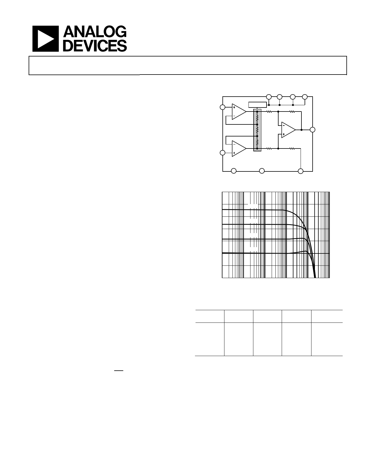
Figure 2. Gain vs. Frequency
10M
100M
Table 1. Instrumentation Amplifiers by Category
General
Purpose
Mil
Zero Drift Grade
Low
Power
High Speed
PGA
AD82201
AD8221
AD8222
AD82241
AD8228
AD82311
AD85531
AD85551
AD85561
AD85571
AD620
AD621
AD524
AD526
AD624
AD6271
AD6231
AD82231
AD8250
AD8251
AD8253
1 Rail-to-rail output.
The AD8251 is available in a 10-lead MSOP package and is
specified over the −40°C to +85°C temperature range, making it
an excellent solution for applications where size and packing
density are important considerations.
Rev. B
Information furnished by Analog Devices is believed to be accurate and reliable. However, no
responsibility is assumed by Analog Devices for its use, nor for any infringements of patents or other
rights of third parties that may result from its use. Specifications subject to change without notice. No
license is granted by implication or otherwise under any patent or patent rights of Analog Devices.
Trademarksandregisteredtrademarksarethepropertyoftheirrespectiveowners.
One Technology Way, P.O. Box 9106, Norwood, MA 02062-9106, U.S.A.
Tel: 781.329.4700
www.analog.com
Fax: 781.461.3113 ©2007–2010 Analog Devices, Inc. All rights reserved.
1 page 
AD8251
Parameter
Settling Time 0.001%
G=1
G=2
G=4
G=8
Slew Rate
G=1
G=2
G=4
G=8
Total Harmonic Distortion + Noise
GAIN
Gain Range
Gain Error
G=1
G = 2, 4, 8
Gain Nonlinearity
G=1
G=2
G=4
G=8
Gain vs. Temperature
INPUT
Input Impedance
Differential
Common Mode
Input Operating Voltage Range
Over Temperature
OUTPUT
Output Swing
Over Temperature
Short-Circuit Current
REFERENCE INPUT
RIN
IIN
Voltage Range
Gain to Output
DIGITAL LOGIC
Digital Ground Voltage, DGND
Digital Input Voltage Low
Digital Input Voltage High
Digital Input Current
Gain Switching Time1
tSU
tHD
t WR -LOW
t WR -HIGH
Conditions
ΔOUT = 10 V step
Min Typ
f = 1 kHz, RL = 10 kΩ, ±10 V,
G = 1, 10 Hz to 22 kHz band-
pass filter
20
30
30
30
G = 1, 2, 4, 8
OUT = ±10 V
1
OUT = −10 V to +10 V
RL = 10 kΩ, 2 kΩ, 600 Ω
RL = 10 kΩ, 2 kΩ, 600 Ω
RL = 10 kΩ, 2 kΩ, 600 Ω
RL = 10 kΩ, 2 kΩ, 600 Ω
All gains
−110
3
Max
785
700
700
770
8
0.03
0.04
9
12
12
15
10
VS = ±5 V to ±15 V
T = −40°C to +85°C
−VS + 1.5
−VS + 1.6
5.3||0.5
1.25||2
T = −40°C to +85°C
−13.5
−13.5
37
+IN, −IN, REF = 0
20
−VS
1 ± 0.0001
Referred to GND
Referred to GND
Referred to GND
−VS + 4.25
DGND
2.8
0
1
See Figure 3 timing diagram
See Figure 3 timing diagram
See Figure 3 timing diagram
See Figure 3 timing diagram
20
10
20
40
+VS − 1.5
+VS − 1.7
+13.5
+13.5
1
+VS
+VS − 2.7
2.1
+VS
325
Unit
ns
ns
ns
ns
V/μs
V/μs
V/μs
V/μs
dB
V/V
%
%
ppm
ppm
ppm
ppm
ppm/°C
GΩ||pF
GΩ||pF
V
V
V
V
mA
kΩ
μA
V
V/V
V
V
V
μA
ns
ns
ns
ns
ns
Rev. B | Page 4 of 24
5 Page 
AD8251
20
15
IB+
10
5
IB–
0
IOS
–5
–10
–60 –40 –20 0
20 40 60 80 100 120 140
TEMPERATURE (ºC)
Figure 18. Input Bias Current and Offset Current vs. Temperature
140
G=4
G=8
120
100 G = 2
80
G=1
60
40
10
140
100 1k 10k
FREQUENCY (Hz)
Figure 19. CMRR vs. Frequency
100k
1M
120
100
G=4
G=2
80 G = 1
G=8
60
40
10 100 1k 10k 100k
FREQUENCY (Hz)
Figure 20. CMRR vs. Frequency, 1 kΩ Source Imbalance
1M
15
10
5
0
–5
–10
–15
–50 –30 –10 10 30 50 70 90 110 130
TEMPERATURE (°C)
Figure 21. ΔCMRR vs. Temperature, G = 1
25
20
15
10
5
0
–5
–10
1k
G=8
G=4
G=2
G=1
VS = ±15V
VIN = 200mV p-p
RL = 2kΩ
10k 100k
1M
FREQUENCY (Hz)
Figure 22. Gain vs. Frequency
10M
100M
40
30
20
10
0
–10
–20
–30
–40
–10 –8 –6 –4 –2 0 2 4 6 8 10
OUTPUT VOLTAGE (V)
Figure 23. Gain Nonlinearity vs. Output Voltage, G = 1, RL = 10 kΩ, 2 kΩ, 600 Ω
Rev. B | Page 10 of 24
11 Page | ||
| Páginas | Total 25 Páginas | |
| PDF Descargar | [ Datasheet AD8251.PDF ] | |
Hoja de datos destacado
| Número de pieza | Descripción | Fabricantes |
| AD825 | Low Cost/ General Purpose High Speed JFET Amplifier | Analog Devices |
| AD8250 | programmable instrumentation amplifier | Analog Devices |
| AD8251 | Programmable Gain Instrumentation Amplifier | Analog Devices |
| AD8253 | Programmable Gain Instrumentation Amplifier | Analog Devices |
| Número de pieza | Descripción | Fabricantes |
| SLA6805M | High Voltage 3 phase Motor Driver IC. |
Sanken |
| SDC1742 | 12- and 14-Bit Hybrid Synchro / Resolver-to-Digital Converters. |
Analog Devices |
|
DataSheet.es es una pagina web que funciona como un repositorio de manuales o hoja de datos de muchos de los productos más populares, |
| DataSheet.es | 2020 | Privacy Policy | Contacto | Buscar |