|
|
|
PDF AD8336 Data sheet ( Hoja de datos )
| Número de pieza | AD8336 | |
| Descripción | DC-Coupled VGA | |
| Fabricantes | Analog Devices | |
| Logotipo | ||
Hay una vista previa y un enlace de descarga de AD8336 (archivo pdf) en la parte inferior de esta página. Total 29 Páginas | ||
|
No Preview Available !
Data Sheet
General-Purpose, −55°C to +125°C,
Wide Bandwidth, DC-Coupled VGA
AD8336
FEATURES
Low noise
Voltage noise: 3 nV/√Hz
Current noise: 3 pA/√Hz
Small-signal BW: 115 MHz
Large-signal BW: 2 V p-p = 80 MHz
Slew rate: 550 V/µs, 2 V p-p
Gain ranges (specified)
−14 dB to +46 dB
0 dB to 60 dB
Gain scaling: 50 dB/V
DC-coupled
Single-ended input and output
Supplies: ±3 V to ±12 V
Temperature range: −55°C to +125°C
Power
150 mW at ±3 V, −55°C < T < +125°C
84 mW at ±3 V, PWRA = 3 V
APPLICATIONS
Industrial process controls
High performance AGC systems
I/Q signal processing
Video
Industrial and medical ultrasound
Radar receivers
GENERAL DESCRIPTION
The AD8336 is a low noise, single-ended, linear in dB, general-
purpose variable gain amplifier, usable over a large range of
supply voltages. It features an uncommitted preamplifier with a
usable gain range of 6 dB to 26 dB. The VGA gain range is 0 dB
to 60 dB, with absolute gain limits of −26 dB to +34 dB. When
the preamplifier gain is adjusted for 12 dB, the combined 3 dB
bandwidth of the preamplifier and VGA is 100 MHz, and the
amplifier is fully usable to 80 MHz. With ±5 V supplies, the
maximum output swing is 7 V p-p.
Because of the X-AMP® architecture, frequency response is
maintained across the entire gain range of the VGA. The differen-
tial gain control interface provides precise linear in dB gain scaling
of 50 dB/V over the temperature span of −55°C to +125°C and
is simple to interface with a variety of external sources.
The large supply voltage range makes the AD8336 suited for
industrial medical applications and video circuits. Dual-supply
operation enables bipolar input signals, such as those generated
by photodiodes or photomultiplier tubes.
The fully independent voltage feedback preamplifier allows both
inverting and noninverting gain topologies. The AD8336 can be
used within the specified gain range of −14 dB to +60 dB by
selecting a preamplifier gain between 6 dB and 26 dB and choosing
appropriate feedback resistors. For the nominal preamplifier gain of
4×, the overall gain range is −14 dB to +46 dB.
If required, quiescent power is limited to a safe level by
asserting the PWRA pin.
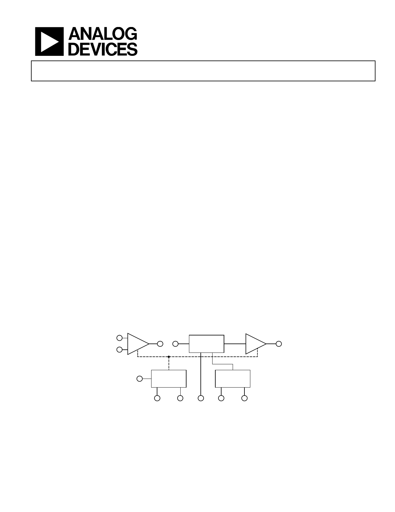
FUNCTIONAL BLOCK DIAGRAM
AD8336
INPP 4
INPN 5
+
PREAMP
–
PRAO VGAI
89
ATTENUATOR
–60dB TO 0dB
34dB
1 VOUT
PWRA 2
BIAS
GAIN CONTROL
INTERFACE
10
VNEG
13
VPOS
3
VCOM
11
GPOS
Figure 1.
12
GNEG
Rev. D
Document Feedback
Information furnished by Analog Devices is believed to be accurate and reliable. However, no
responsibilityisassumedbyAnalogDevices for itsuse,nor foranyinfringementsofpatentsor other
rights of third parties that may result from its use. Specifications subject to change without notice. No
license is granted by implication or otherwise under any patent or patent rights of Analog Devices.
Trademarksandregisteredtrademarksarethepropertyoftheirrespectiveowners.
One Technology Way, P.O. Box 9106, Norwood, MA 02062-9106, U.S.A.
Tel: 781.329.4700 ©2006–2016 Analog Devices, Inc. All rights reserved.
Technical Support
www.analog.com
1 page 
AD8336
Data Sheet
Parameter
ABSOLUTE GAIN ERROR2
GAIN CONTROL INTERFACE
Gain Scaling Factor
Intercept
Gain Range
Input Voltage (VGAIN) Range
Input Current
Response Time
OUTPUT PERFORMANCE
Output Impedance, DC to 10 MHz
Output Signal Swing
Output Current
Short-Circuit Current
Output Offset Voltage
PWRA PIN
Normal Power (Logic Low)
Low Power (Logic High)
Normal Power (Logic Low)
Low Power (Logic High)
Normal Power (Logic Low)
Low Power (Logic High)
POWER SUPPLY
Supply Voltage Operating Range
Quiescent Current
VS = ±3 V
VS = ±5 V
VS = ±12 V
Power Dissipation
Power Supply Rejection Ratio (PSRR)
Test Conditions/Comments
−0.7 V < VGAIN < −0.6 V
−0.6 V < VGAIN < −0.5 V
−0.5 V < VGAIN < +0.5 V
−0.5 V < VGAIN < +0.5 V, ±3 V ≤ VS ≤ ±12 V
−0.5 V < VGAIN < +0.5 V, −55°C ≤ T ≤ +125°C
−0.5 V < VGAIN < +0.5 V, preamplifier gain = −3×
0.5 V < VGAIN < +0.6 V
0.6 V < VGAIN < +0.7 V
Preamplifier + VGA
VGA only
No foldover
60 dB gain change
±3 V ≤ VS ≤ ±12 V
RL ≥ 500 Ω (for |VS| ≤ ±5 V); RL ≥ 1 kΩ above that
RL ≥ 1 kΩ (for |VS| = ±12 V)
Linear operation − minimum discernable distortion
VS = ±3 V
VS = ±5 V
VS = ±12 V
VGAIN = 0.7 V, gain = 200×
±3 V ≤ VS ≤ ±12 V
−55°C ≤ T ≤ +125°C
VS = ±3 V
VS = ±3 V
VS = ±5 V
VS = ±5 V
VS = ±12 V
VS = ±12 V
−55°C ≤ T ≤ +125°C
PWRA = 3 V
−55°C ≤ T ≤ +125°C
PWRA = 5 V
−55°C ≤ T ≤ +125°C
PWRA = 5 V
VS = ±3 V
VS = ±5 V
VS = ±12 V
VGAIN = 0.7 V, f = 1 MHz
1 All dBm values are calculated with 50 Ω reference, unless otherwise noted.
2 Conformance to theoretical gain expression (see the Setting the Gain section).
Min
0
0
−1.25
−4.0
−9.0
Typ
1 to 5
0.5 to 1.5
±0.2
±0.5
±0.5
±0.5
−1.5 to −3.0
−1 to −5
48 49.9
16.4
4.5
58 60
−VS
1
300
−250
2.5
|VS| − 1.5
|VS| − 2.25
20
+123/−72
+123/−72
+72/−73
−125
−200
−200
1.5
2.0
4.0
±3
22 25
23 to 31
10 14
22 26
23 to 31
10 14
23 28
24 to 33
16
150
260
672
−40
Max
6
3
+1.25
+1.25
0
0
52
62
+VS
+150
0.7
1.2
3.2
±12
30
18
30
18
31
Unit1
dB
dB
dB
dB
dB
dB
dB
dB
dB/V
dB
dB
dB
V
μA
ns
Ω
V
V
mA
mA
mA
mA
mV
mV
mV
V
V
V
V
V
V
V
mA
mA
mA
mW
mW
mW
dB
Rev. D | Page 4 of 28
5 Page 
AD8336
50
VGAIN = +0.7V
40 +0.5V
30
+0.2V
20
0V
10
–0.2V
0
–10 –0.5V
–0.7V
–20
–30
100k
PREAMP GAIN = –3×
1M 10M
FREQUENCY (Hz)
100M 200M
Figure 21. Frequency Response for Various Values of VGAIN
When the Preamplifier Gain is −3×
(See Figure 69 and Figure 57)
25
VGAIN = 0V
20
15
10
5
0
–5
–10
100k
CL = 47pF
CL = 22pF
CL = 10pF
CL = 0pF
1M 10M
FREQUENCY (Hz)
100M 200M
Figure 22. Frequency Response for Various Values of Load Capacitance (CL)
(See Figure 57)
30
GAIN = 20×
25
20
15 GAIN = 4×
10
5
0
–5
–10
100k
VS = ±12V
VS = ±5V
VS = ±3V
1M
10M
FREQUENCY (Hz)
100M
500M
Figure 23. Preamplifier Frequency Response for Three Values of Supply
Voltage (VS) When the Preamplifier Gain is 4× or 20×
(See Figure 58)
Data Sheet
30
25
20 GAIN = –19×
15
GAIN = –3×
10
5
0
–5 VS = ±12V
VS = ±5V
–10 VS = ±3V
100k
1M
10M
FREQUENCY (Hz)
100M
500M
Figure 24. Preamplifier Frequency Response for Three Values of Supply
Voltage (VS) When the Inverting Gain Value is −3× or −19×
(See Figure 69)
20
PREAMP GAIN = 20×
PREAMP GAIN = 4×
15
10
5
0
1M 10M 100M
FREQUENCY (Hz)
Figure 25. Group Delay vs. Frequency for Preamplifier Gains of 4× and 20×
(See Figure 59)
1k
100
10
1
0.1
0.01
100k
1M 10M
FREQUENCY (Hz)
100M
500M
Figure 26. Output Resistance vs. Frequency of the Preamplifier
(See Figure 61)
Rev. D | Page 10 of 28
11 Page | ||
| Páginas | Total 29 Páginas | |
| PDF Descargar | [ Datasheet AD8336.PDF ] | |
Hoja de datos destacado
| Número de pieza | Descripción | Fabricantes |
| AD8330 | Variable Gain Amplifier | Analog Devices |
| AD8331 | Ultralow Noise VGAs | Analog Devices |
| AD8332 | Ultralow Noise VGAs | Analog Devices |
| AD8333 | Dual I/Q Demodulator and Phase Shifter | Analog Devices |
| Número de pieza | Descripción | Fabricantes |
| SLA6805M | High Voltage 3 phase Motor Driver IC. |
Sanken |
| SDC1742 | 12- and 14-Bit Hybrid Synchro / Resolver-to-Digital Converters. |
Analog Devices |
|
DataSheet.es es una pagina web que funciona como un repositorio de manuales o hoja de datos de muchos de los productos más populares, |
| DataSheet.es | 2020 | Privacy Policy | Contacto | Buscar |