|
|
|
PDF AD5378 Data sheet ( Hoja de datos )
| Número de pieza | AD5378 | |
| Descripción | Bipolar Voltage Output DAC | |
| Fabricantes | Analog Devices | |
| Logotipo | ||
Hay una vista previa y un enlace de descarga de AD5378 (archivo pdf) en la parte inferior de esta página. Total 28 Páginas | ||
|
No Preview Available !
www.DataSheet4U.com
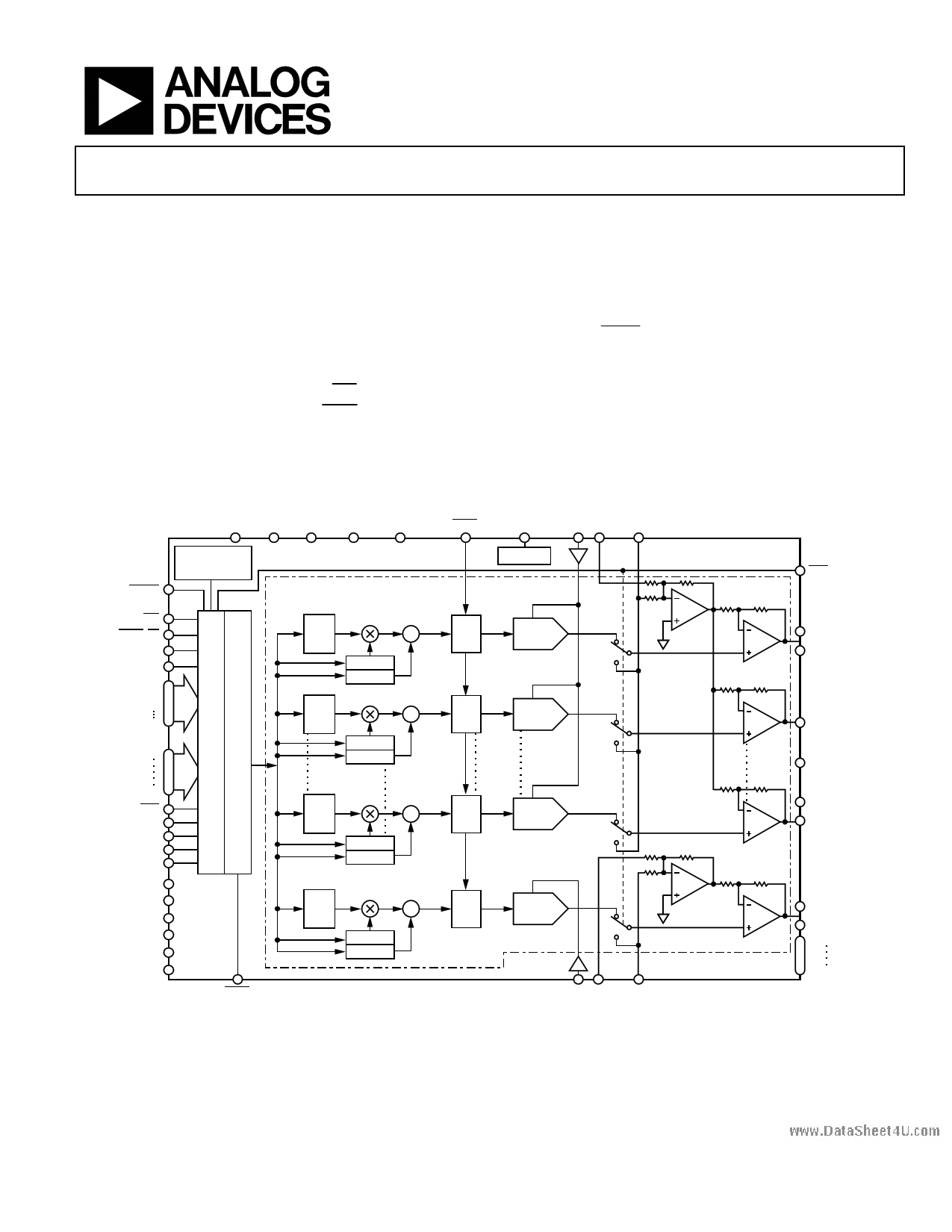
32-Channel, 14-Bit, Parallel and
Serial Input, Bipolar Voltage Output DAC
Preliminary Technical Data
AD5378
FEATURES
32-channel DAC in 13 mm × 13 mm 108-lead CSPBGA
Guaranteed monotonic to 14 bits
Buffered voltage outputs
Output voltage span of 3.5 V × VREF(+)
Maximum output voltage span of 17.5 V
System calibration function allowing user-programmable
offset and gain
Pseudo differential outputs relative to REFGND
Clear function to user-defined REFGND (CLR pin)
Simultaneous update of DAC outputs (LDAC pin)
DAC increment/decrement mode
Channel grouping and addressing features
Interface options
Parallel interface
DSP/microcontroller-compatible 3-wire serial interface
2.5 V to 5.5 V JEDEC-compliant digital levels
SDO daisy-chaining option
Power-on reset
Digital reset (RESET pin and soft reset function)
APPLICATIONS
Level setting in automatic test equipment (ATE)
Variable optical attenuators (VOAs)
Optical switches
Industrial control systems
FUNCTIONAL BLOCK DIAGRAM
VCC
VDD VSS AGND
DGND
LDAC
VBIAS VREF1(+) VREF1(–) REFGND A1
RESET
POWER-ON
RESET
AD5378
VBIAS
DCEN/WR
SYNC/CS
REG0
REG1
DB13
SCLK/DB12
DIN/DB11
DB0
A7
/ /14
INPUT
REG
14
0–1
m REG0–1
/14
c REG0–1
/ /14 INPUT 14
REG
2
m REG2
14/ /14 c REG2
/ /14
DAC
REG
14
DAC 0–1
0–1
/ /14
DAC 14
REG
DAC 2
2
A0
SER/PAR
DIN
SCLK
SDO
FIFOEN
REFGND B1
REFGND B2
REFGND C1
REFGND C2
REFGND D1
REFGND D2
/ /14
INPUT
REG
14
5
m REG7
/14 c REG7
/ /14
DAC
REG
14
DAC 5
5
BUSY
/ /14
INPUT
REG
14
6–7
m REG8–9
/14 c REG8–9
/ /14
DAC
REG
14
DAC 6–7
6–7
×4
VREF2(+) VREF2(–) REFGND A2
Figure 1.
Protected by U.S. Patent No. 5,969,657 and 6,823,416; other patents pending.
CLR
VOUT 0
VOUT 1
VOUT 2
VOUT 3
VOUT 4
VOUT 5
VOUT 6
VOUT 7
VOUT 8
VOUT 31
Rev. PrA
Information furnished by Analog Devices is believed to be accurate and reliable.
However, no responsibility is assumed by Analog Devices for its use, nor for any
infringements of patents or other rights of third parties that may result from its use.
Specifications subject to change without notice. No license is granted by implication
or otherwise under any patent or patent rights of Analog Devices. Trademarks and
registered trademarks are the property of their respective owners.
DataSheet4 U .com
One Technology Way, P.O. Box 9106, Norwood, MA 02062-9106, U.S.A.
Tel: 781.329.4700
www.analog.com
Fax: 781.326.8703 © 2005 Analog Devices, Inc. All rights reserved.
1 page 
www.DataSheet4U.com
Preliminary Technical Data
Parameter
POWER REQUIREMENTS
VCC
VDD
VSS
Power Supply Sensitivity2
∆ Full Scale/∆ VDD
∆ Full Scale/∆ VSS
∆ Full Scale/∆ VCC
ICC
IDD
ISS
Power Dissipation
Power Dissipation Unloaded (P)
Power Dissipation Loaded (PTOTAL)
Junction Temperature
A Version1
2.7/5.5
8.5/16.5
−3/−16.5
−75
−75
−90
5
28
23
850
2000
130
Unit
V min/max
V min/max
V min/max
dB typ
dB typ
dB typ
mA max
mA max
mA max
mW max
mW max
°C max
1 Temperature range for the A version: −40°C to +85°C. Typical specifications are at 25°C.
2 Guaranteed by design and characterization; not production tested.
3 Where θJ represents the package thermal impedance.
Test Conditions/Comments
AD5378
VCC = 5.5 V, VIH = VCC, VIL = GND
Outputs unloaded; typically 20 mA
Outputs unloaded; typically 15 mA
VDD = 16.5 V, VSS = −16.5 V
PTOTAL = P + Σ(VDD − VO) × ISOURCE + Σ(VO − VSS) × ISINK
TJ = TA + PTOTAL × θJ3
AC CHARACTERISTICS
VCC = 2.7 V to 5.5 V; VDD = 11.4 V to 16.5 V; VSS = −11.4 V to −16.5 V; VREF(+) = +5 V; VREF(−) = −3.5 V;
AGND = DGND = REFGND = 0 V; VBIAS = 5 V; CL = 220 pF; RL = 11 kΩ to 3 V; gain = 1; offset = 0 V.
Table 4.
Parameter
DYNAMIC PERFORMANCE
Output Voltage Settling Time
Slew Rate
Digital-to-Analog Glitch Energy
Glitch Impulse Peak Amplitude
Channel-to-Channel Isolation
DAC-to-DAC Crosstalk
Digital Crosstalk
Digital Feedthrough
Output Noise Spectral Density @ 1 kHz
A Version1
20
30
1
20
15
100
40
10
0.1
1
350
Unit
µs typ
µs max
V/µs typ
nV-s typ
mV max
dB typ
nV-s typ
nV-s typ
nV-s typ
nV-s typ
nV/(Hz)1/2 typ
Test Conditions/Comments
Full-scale change to ±1/2 LSB
DAC latch contents alternately loaded with all 0s and
all 1s
VREF(+) = 2 V p-p, (1 VBIAS) 1 kHz, VREF(−) = −1 V
See the Terminology section; between DACs inside a
group
Between DACs from different groups
Effect of input bus activity on DAC output under test
VREF(+) = VREF(−) = 0 V
1 Guaranteed by design and characterization; not production tested.
DataSheet4 U .com
Rev. PrA | Page 5 of 28
5 Page 
www.DataSheet4U.com
Preliminary Technical Data
ABSOLUTE MAXIMUM RATINGS
TA = 25°C, unless otherwise noted.
Transient currents of up to 100 mA do not cause SCR latch-up.
Table 7.
Parameter
VDD to AGND
VSS to AGND
VCC to DGND
Digital Inputs to DGND
Digital Outputs to DGND
VREF1(+), VREF2(+) to AGND
VREF1(−), VREF2(−) to AGND
VBIAS to AGND
VOUT0–VOUT31 to AGND
REFGND to AGND
AGND to DGND
Operating Temperature Range (TA)
Industrial (A Version)
Storage Temperature Range
Junction Temperature (TJ max)
108-Lead CSPBGA Package
θJA Thermal Impedance
θJC Thermal Impedance
Reflow Soldering
Peak Temperature
Time at Peak Temperature
Rating
−0.3 V to +17 V
−17 V to +0.3 V
−0.3 V to +7 V
−0.3 V to VCC + 0.3 V
−0.3 V to VCC + 0.3 V
−0.3 V to +7 V
VSS − 0.3 V to VDD + 0.3 V
−0.3 V to +7 V
VSS − 0.3 V to VDD + 0.3 V
VSS − 0.3 V to VDD + 0.3 V
−0.3 V to +0.3 V
−40°C to +85°C
−65°C to +150°C
150°C
37.5°C/W
8.5°C/W
230°C
10 sec to 40 sec
AD5378
Stresses above those listed under Absolute Maximum Ratings
may cause permanent damage to the device. This is a stress
rating only; functional operation of the device at these or any
other conditions above those listed in the operational sections
of this specification is not implied. Exposure to absolute
maximum rating conditions for extended periods may affect
device reliability. Only one absolute maximum rating may be
applied at any one time.
ESD CAUTION
ESD (electrostatic discharge) sensitive device. Electrostatic charges as high as 4000 V readily accumulate on
the human body and test equipment and can discharge without detection. Although this product features
proprietary ESD protection circuitry, permanent damage may occur on devices subjected to high energy
electrostatic discharges. Therefore, proper ESD precautions are recommended to avoid performance
degradation or loss of functionality.
DataSheet4 U .com
Rev. PrA | Page 11 of 28
11 Page | ||
| Páginas | Total 28 Páginas | |
| PDF Descargar | [ Datasheet AD5378.PDF ] | |
Hoja de datos destacado
| Número de pieza | Descripción | Fabricantes |
| AD537 | Integrated Circuit Voltage-to-Frequency Converter | Analog Devices |
| AD5370 | Voltage-Output DACs | Analog Devices |
| AD5371 | Voltage-Output DAC | Analog Devices |
| AD5372 | (AD5372 / AD5373) Voltage-Output DACs | Analog Devices |
| Número de pieza | Descripción | Fabricantes |
| SLA6805M | High Voltage 3 phase Motor Driver IC. |
Sanken |
| SDC1742 | 12- and 14-Bit Hybrid Synchro / Resolver-to-Digital Converters. |
Analog Devices |
|
DataSheet.es es una pagina web que funciona como un repositorio de manuales o hoja de datos de muchos de los productos más populares, |
| DataSheet.es | 2020 | Privacy Policy | Contacto | Buscar |