|
|
|
PDF ADAU1701 Data sheet ( Hoja de datos )
| Número de pieza | ADAU1701 | |
| Descripción | SigmaDSP 28/56-Bit Audio Processor | |
| Fabricantes | Analog Devices | |
| Logotipo | ||
Hay una vista previa y un enlace de descarga de ADAU1701 (archivo pdf) en la parte inferior de esta página. Total 43 Páginas | ||
|
No Preview Available !
www.DataSheet4U.com
Preliminary Technical Data
FEATURES
28/56-bit, 50 MHz digital audio processor
Stereo ADC: 100 dB SNR and -80 dB THD+N
4-channel DAC: 104 dB SNR and -90 dB THD+N
Complete stand-alone operation
• Self-boot from serial EEPROM
• Auxiliary ADC with four-input mux for analog
control
• GPIOs for digital controls and outputs
Fully programmable with SigmaStudio™ graphical tool
28-bit × 28-bit multiplier with 56-bit accumulator for full
double precision processing
Clock Oscillator for generating master clock from crystal
PLL for generating master clock from 64 × fS, 256 × fS,
384 × fS, or 512 × fS clocks
Flexible serial data I/O ports with I2S compatible, left-
justified, right-justified, and TDM modes
Sampling rates up to 192 kHz supported
On-chip voltage regulator for compatibility with 3.3 V
systems
48-lead LQFP plastic package
GENERAL DESCRIPTION
The ADAU1701 is a complete audio system-on-a-chip
including a 28/56-bit audio DSP, ADCs and DACs, and
microcontroller-like control interfaces. Signal processing
includes equalization, crossover, bass enhancement, multiband
dynamics processing, delay compensation, speaker
compensation, and stereo image widening. These algorithms
can be used to compensate for the real-world limitations of
speakers, amplifiers, and listening environments, resulting in a
dramatic improvement of perceived audio quality.
The signal processing used in the ADAU1701 is comparable to
that found in high end studio equipment. Most of the
processing is done in full 56-bit double-precision mode,
resulting in very good low level signal performance. The
ADAU1701 is a fully-programmable DSP. The easy-to-use
SigmaStudio software allows the user to graphically configure a
custom signal processing flow using blocks such as biquad
Rev. PrF
Information furnished by Analog Devices is believed to be accurate and reliable. However, no
responsibility is assumed by Analog Devices for its use, nor for any infringements of patents or other
rights of third parties that may result from its use. Specifications subject to change without notice. No
license is granted by implication or otherwise under any patent or patent rights of Analog Devices.
Trademarksandregisteredtrademarksarethepropertyoftheirrespectiveowners.
DataSheet4 U .com
SigmaDSP® 28/56-Bit Audio
Processor with 2ADC/4DAC
ADAU1701
APPLICATIONS
Multimedia speaker systems
MP3 player speaker docks
Automotive head units
Mini-component stereos
Digital televisions
Studio monitors
Speaker crossovers
Musical instrument effects processors
In-seat sound systems (aircraft/motor coaches)
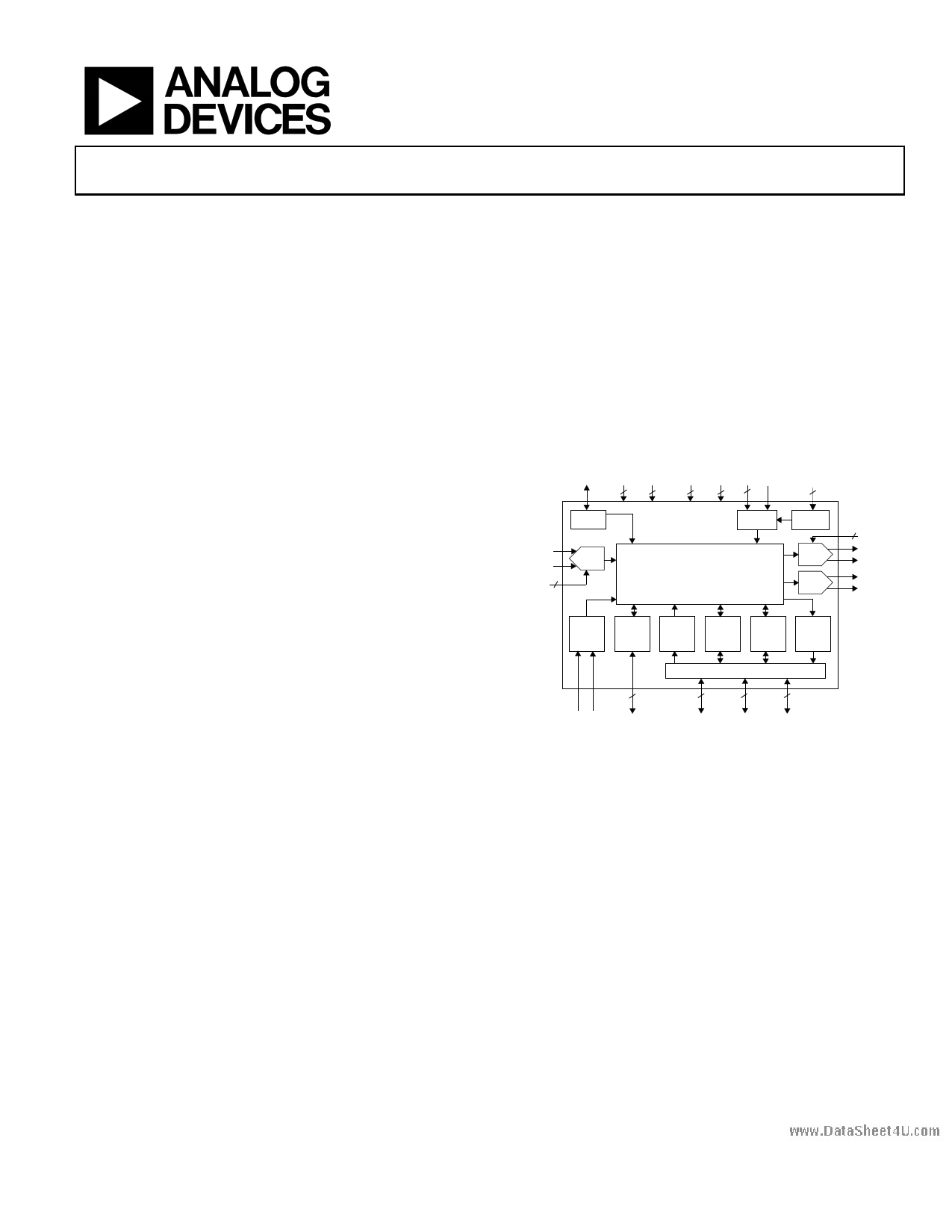
FUNCTIONAL BLOCK DIAGRAM
PLL
DIGITAL DIGITAL ANALOG ANALOG PLL LOOP
3.3 V
VDD GROUND
VDD GROUND MODE FILTER
CRYSTAL
33
3 33
2
1.8 V
REGULATOR
2-CHANNEL
ANALOG
INPUT
FILTA /
ADC_RES 2
STEREO
ADC
PLL
S
28/56-BIT, 50 MHz
AUDIO PROCESSOR CORE
40 ms DELAY MEMORY
CLOCK
OSCILLATOR
DAC
DAC
RESET/
MODE
SELECT
CONTROL
INTERFACE
AND
SELFBOOT
8-CH
DIGITAL
INPUT
8-BIT
AUX
ADC
GPIO
8-CH
DIGITAL
OUTPUT
INPUT/OUTPUT MATRIX
RESET SELF
BOOT
5
I2C/SPI &
WRITEBACK
44
DIGITAL IN
OR
GPIO
AUX ADC
OR
GPIO
Figure 1.
4
DIGITAL OUT
OR
GPIO
FILTD / CM
2
4-CHANNEL
ANALOG
OUTPUT
filters, dynamics processors, level controls, and GPIO interface
controls.
ADAU1701 programs can be loaded on power-up either from a
serial EEPROM though its own self-boot mechanism or from
an external microcontroller. On power-down, the current state
of the parameters can be written back to the EEPROM from the
ADAU1701 to be recalled the next time the program is run.
The ADAU1701’s two sigma-delta (Σ-Δ ) ADCs and four Σ-Δ
DACs provide an analog-in to analog-out dynamic range
greater than 100 dB. The ADC’s THD+N is -80 dB and the
DAC’s is -90 dB. Digital input and output ports allow a glueless
connection to additional ADCs and DACs. The ADAU1701
communicates through either an I2C bus or a 4-wire SPI port.
One Technology Way, P.O. Box 9106, Norwood, MA 02062-9106, U.S.A.
Tel: 781.329.4700
www.analog.com
Fax: 781.461.3113
©2006 Analog Devices, Inc. All rights reserved.
1 page 
www.DataSheet4U.com
Preliminary Technical Data
ADAU1701
Parameter
Gain Error
DC Bias
Power Supply Rejection
Min
DIGITAL I/O
Table 3. Digital I/O
Parameter
Input Voltage, HI (VIH)
Input Voltage, LO (VIL)
Input Leakage, HI (IIH)
Input Leakage, LO (IIL)
High Level Output Voltage (VOH), IOH = 1 mA
Low Level Output Voltage (VOL), IOL = 1 mA
Input Capacitance
GPIO Output Drive
POWER
Table 4.
Parameter
Supply Voltage
Analog Voltage
Digital Voltage
PLL Voltage
IOVDD Voltage
Supply Current
Analog Current (AVDD & PVDD)
Digital Current (DVDD)
PLL Current
Analog Current, Reset
Digital Current, Reset
PLL Current, Reset
Dissipation
Operation (AVDD, DVDD, PVDD)2
Reset, all supplies
Typical
TBD
1.5
TBD
Max
Comments
Units
%
V
dB
Test Conditions/Comments
1kHz, 300mVP-P Signal at AVDD
Min Typ Max
2.0 IOVDD
0.8
10
10
2.0
0.8
5
5
Min Typ Max1
3.3
1.8
3.3
3.3
65 85
40 60
TBD
TBD
TBD
TBD
286.5
TBD
1 Maximum specifications are measured across −xx°C to xx°C (case) and across VDD = xxx V to xxx V.
2 Power dissipation does not include IOVDD power because the current draw from this supply is dependant on loads on the digital output pins.
TEMPERATURE RANGE
Table 5.
Parameter
Min Typ Max Unit
Functionality Guaranteed
0°C
70°C °C Ambient
DIGITAL TIMING
Table 6 Digital Timing1
Parameter
MASTER CLOCK
tMP MCLK Period
tMP MCLK Period
tMP MCLK Period
tMP MCLK Period
SERIAL PORT
tBIL INPUT_BCLK LO Pulse Width
tBIH INPUT_BCLK HI Pulse Width
tLIS INPUT_LRCLK Setup
tLIH INPUT_LRCLK Hold
Comments
512 fS mode
384 fS mode
256 fS mode
64 fS mode
To INPUT_BCLK rising
From INPUT_BCLK rising
Min Max
36 244
48 366
73 488
291 1953
40
40
10
10
Rev. PrF | Page 5 of 43
Unit
V
V
μA
μA
V
V
pF
mA
Unit
V
V
V
V
mA
mA
mA
mA
mA
mA
mW
mW
Unit
ns
ns
ns
ns
ns
ns
ns
ns
DataSheet4 U .com
5 Page 
www.DataSheet4U.com
Preliminary Technical Data
ADAU1701
DGND with a 100 nF capacitor.
14 D_IO MP7
Multi-Purpose – GPIO or Serial output port data 1 (SDATA_OUT1)
15 D_IO MP6
Multi-Purpose – GPIO, Serial output port data 0, or TDM data output
(SDATA_OUT0)
16 D_IO MP10
Multi-Purpose – GPIO or Serial output port LRCLK (OUTPUT_LRCLK)
17 A_OUT VDRIVE
Drive for 1.8 V regulator. The base of the voltage regulator’s external PNP
transistor is driven from VDRIVE.
18 PWR IOVDD
Input and Output pins supply. The voltage on this pin sets the highest input
voltage that should be seen on the digital input pins. This pin is also the supply
for the digital output signals on the control port and MP pins. IOVDD should
always be set to 3.3 V. The current draw of this pin is variable because it is
dependant on the loads of the digital outputs.
19 D_IO MP11
Multi-Purpose – GPIO or Serial output port BCLK (OUTPUT_BCLK)
20 D_IN ADDR1/CDATA/WB ADDR1: I2C Address 1, in combination with ADDR0 it will set the I2C address of
the IC. Four ADAU1701s to be used on the same I2C bus.
CDATA: SPI Data Input
WB: EEPROM Writeback trigger. A rising (default) or falling (if set in the EEPROM
messages) edge on this pin will trigger a write-back of the interface registers to
the external EEPROM. This function can be used to save parameter data on
power-down.
21 D_IN CLATCH / WP
CLATCH: This SPI latch signal must go low at the beginning of an SPI transaction
and high at the end of a transaction. Each SPI transaction may take a different
number of CCLKs to complete, depending on the address and read/write bit that
are sent at the beginning of the SPI transaction.
WP: Self-boot EEPROM write protect. This pin is an open collector output when in
selfboot mode. The ADAU1701 will pull this low to prohibit writes to an external
EEPROM. This pin should be pulled high to 3.3 V.
22 D_IO SDA/COUT
SDA: This I2C data pin is a bidirectional open collector. The line connected to this
pin should have a 2.2 kΩ pull-up resistor.
COUT: This SPI data output is used for reading back registers and memory
locations. It is three-stated when an SPI read is not active.
23 D_IO SCL/CCLK
SCL: This I2C clock pin is always an open collector input when in I2C control mode.
In self-boot mode this pin will be an open collector output (I2C master). The line
connected to this pin should have a 2.2 kΩ pull-up resistor.
CCLK: This SPI clock may either run continuously or be gated off in between SPI
transactions.
24 PWR DVDD
1.8 V Digital Supply. This can be supplied either externally or generated from a
3.3 V supply with the on-board 1.8 V regulator. DVDD should be decoupled to
DGND with a 100 nF capacitor.
25 PWR DGND
DGND is a digital ground pin. The AGND, DGND, and PGND pins can be tied
directly together in a common ground plane. dGND should be decoupled to a
DVDD pin with a 100 nF capacitor.
26 D/A_IO MP9
Multi-Purpose – GPIO, serial output port data 3 (SDATA_OUT3), or auxiliary ADC
input 0
27 D/A_IO MP8
Multi-Purpose – GPIO, serial output port data 2 (SDATA_OUT2), or auxiliary ADC
input 3
28 D/A_IO MP3
Multi-Purpose – GPIO, serial input port data 3 (SDATA_IN3), or auxiliary ADC
input 2
29 D/A_IO MP2
Multi-Purpose – GPIO, serial input port data 2 (SDATA_IN2), or auxiliary ADC
input 1
30 X RSVD
Reserved, tie to ground, either directly or through a pull-down resistor.
31 D_OUT OSCO
OSCO is the output of the crystal oscillator circuit. A 100 Ω damping resistor
should be connected between this pin and the crystal. This output should not be
used to directly drive a clock to another IC. If the crystal oscillator is not used, this
pin can be left unconnected.
32 D_IN MCLKI
MCLKI can either be connected to a 3.3 V clock signal or can be the input from
the crystal oscillator circuit.
33 PWR PGND
PGND is the PLL ground pin. The AGND, DGND, and PGND pins can be tied
directly together in a common ground plane. PGND should be decoupled to
Rev. PrF | Page 11 of 43
DataSheet4 U .com
11 Page | ||
| Páginas | Total 43 Páginas | |
| PDF Descargar | [ Datasheet ADAU1701.PDF ] | |
Hoja de datos destacado
| Número de pieza | Descripción | Fabricantes |
| ADAU1701 | SigmaDSP 28/56-Bit Audio Processor | Analog Devices |
| ADAU1702 | SigmaDSP 28-56-Bit Audio Processor | Analog Devices |
| Número de pieza | Descripción | Fabricantes |
| SLA6805M | High Voltage 3 phase Motor Driver IC. |
Sanken |
| SDC1742 | 12- and 14-Bit Hybrid Synchro / Resolver-to-Digital Converters. |
Analog Devices |
|
DataSheet.es es una pagina web que funciona como un repositorio de manuales o hoja de datos de muchos de los productos más populares, |
| DataSheet.es | 2020 | Privacy Policy | Contacto | Buscar |