|
|
PDF DS1857 Data sheet ( Hoja de datos )
| Número de pieza | DS1857 | |
| Descripción | Dual Temperature-Controlled Resistors with External Temperature Input and Monitors | |
| Fabricantes | Maxim Integrated Products | |
| Logotipo |  |
|
Hay una vista previa y un enlace de descarga de DS1857 (archivo pdf) en la parte inferior de esta página. Total 22 Páginas | ||
|
No Preview Available !
www.DataSheet4U.com
Rev 1; 6/04
Dual Temperature-Controlled Resistors with
External Temperature Input and Monitors
General Description
Features
The DS1857 dual temperature-controlled nonvolatile
(NV) variable resistors with external temperature input
and monitors consists of two 50kΩ 256-position linear
variable resistors, two analog monitor inputs (MON1,
MON2), and an external temperature sensor input. The
device provides an ideal method for setting and tem-
perature-compensating bias voltages and currents in
control applications using minimal circuitry. The vari-
able resistor settings are stored in EEPROM memory
and can be accessed over the 2-wire serial bus.
♦ Four Total Monitored Channels (Temperature,
VCC, MON1, MON2)
♦ Two External Analog Inputs (MON1, MON2)
♦ Interface to External Temperature Sensor (LM50)
♦ Two 50kΩ, Linear, 256-Position, Nonvolatile
Temperature-Controlled Variable Resistors
♦ Resistor Settings Changeable Every 2°C
♦ Access to Monitoring and ID Information
Configurable with Separate Device Addresses
♦ Resistor Disable (Open-Circuit) Function
♦ 2-Wire Serial Interface
♦ Three Address Lines for Multiple Devices
Optical Transceivers
Applications
♦ Operates from a 3.3V or 5V Supply
♦ SFF-8472 Compatible
Optical Transponders
Instrumentation and Industrial Controls
Ordering Information
RF Power Amps
Diagnostic Monitoring
PART
www.DataSheDeSt148U57.Ec-o05m0
TEMP RANGE PIN-PACKAGE
-40°C to +95°C 16 TSSOP
DS1857E-050/T&R
-40°C to +95°C
16 TSSOP
(Tape-and-Reel)
DS1857B-050
-40°C to +95°C 16 Ball CSBGA
Typical Operating Circuit
VCC
VCC = 3.3V
4.7kΩ
4.7kΩ
2-WIRE
INTERFACE
VCC
1 SDA
2 SCL
3 A0**
4 A1**
GROUND TO
DISABLE WRITE
PROTECT
Tx DISABLE
5 A2**
6 WPEN
7 RHIZ
8 GND
VCC 16
0.1µF
DECOUPLING
CAP
15
H1
14
L1
TO LASER BIAS
CONTROL
DS1857
13
H0
12
L0
TO LASER MODULATION
CONTROL
11
EXTTMP
TO EXTERNAL TEMPERATURE
SENSOR, SUCH AS LM50
MON2 10 Rx POWER* DIAGNOSTIC
MON1 9 Tx BIAS*
INPUTS
0 TO 2.5V FS
*Rx POWER AND Tx BIAS CAN BE ARBITRARILY
ASSIGNED TO THE MON INPUTS.
**ADDRESS INPUTS DETERMINE THE MAIN DEVICE 2-WIRE
SLAVE ADDRESS WHEN ADFIX = 0. THIS ADDRESS MUST BE
DIFFERENT THAN THE AUX DEVICE ADDRESS WHEN ADEN = 0.
Pin Configurations
TOP VIEW
A A1 SCL VCC H1
B A2 SDA H0
L1
C RHIZ WPEN A0 EXTTMP
D GND L0 MON1 MON2
1234
16-BALL CSBGA (4mm x 4mm)
1.0mm PITCH
1 SDA
2 SCL
3 A0
4 A1
5 A2
6 WPEN
7 RHIZ
8 GND
VCC 16
H1 15
L1 14
DS1857
H0 13
L0 12
EXTTMP 11
MON2 10
MON1 9
16 TSSOP
______________________________________________ Maxim Integrated Products 1
For pricing delivery, and ordering information please contact Maxim/Dallas Direct! at
1-888-629-4642, or visit Maxim’s website at www.maxim-ic.com.
www.DataSheet4U.com
1 page 
www.DataSheet4U.com
Dual Temperature-Controlled Resistors with
External Temperature Input and Monitors
AC ELECTRICAL CHARACTERISTICS (continued)
(VCC = 3.0V to 5.5V, TA = -40°C to +95°C, unless otherwise noted.)
Note 11: After this period, the first clock pulse is generated.
Note 12: The maximum tHD:DAT only to has be met if the device does not stretch the LOW period (tLOW) of the SCL signal.
Note 13: A device must internally provide a hold time of at least 300ns for the SDA signal (see the VIH MIN of the SCL signal) in order
to bridge the undefined region of the falling edge of SCL.
Note 14: CB—total capacitance of one bus line, timing referenced to 0.9 x VCC and 0.1 x VCC.
Note 15: EEPROM write begins after a STOP condition occurs.
(VCC = 5.0V, TA = +25°C, unless otherwise noted.)
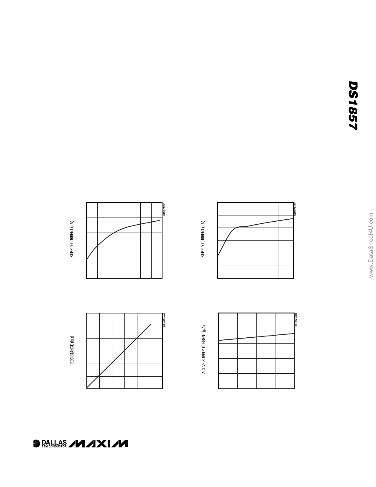
Typical Operating Characteristics
SUPPLY CURRENT vs. TEMPERATURE
700
SUPPLY CURRENT vs. VOLTAGE
700
660 650
600
620
www.DataSheet4U55.0com
580
500
540 450
500
-40 -20
0 20 40 60
TEMPERATURE (°C)
80 100
RESISTANCE vs. SETTING
60
50
40
30
20
10
400
3.0 3.5 4.0 4.5 5.0
VOLTAGE (V)
ACTIVE SUPPLY CURRENT
vs. SCL FREQUENCY
700
SDA = 5V
660
5.5
620
580
540
0
0 50 100 150 200 250 300
SETTING
500
0
100 200 300
SCL FREQUENCY (kHz)
400
www.DataSheet4U.com
_____________________________________________________________________ 5
5 Page 
www.DataSheet4U.com
Dual Temperature-Controlled Resistors with
External Temperature Input and Monitors
Variable Resistors ADFIX (address fixed) determines whether the Main
The value of each variable resistor is determined by a Device address is determined by an EEPROM byte
temperature-addressed look-up table, which can (Table 01, byte 8Ch, when ADFIX =1). There can be up
assign a unique value (00h to FFh) to each resistor for to 128 devices sharing a common 2-wire bus, with
every 2°C increment over the -40°C to +102°C range each device having its own unique device address.
(see Table 3). See the Temperature Conversion section
for more information.
A resistor disable feature places both outputs in a high-
impedance mode. This occurs when the RHIZ input is
high. An internal pullup of RRHIZ is provided, readying
this pin for input from the Tx Disable signal as specified
in the SFF and SFP MSA.
Memory Protection
Memory access from either device address can be
either read/write or read only. Write protection is
accomplished by a combination of control bits in
EEPROM (APEN and MPEN in configuration register
89h) and a write-protect enable (WPEN) pin. Since the
WPEN pin is often not accessible from outside the mod-
The variable resistors can also be used in manual ule, this scheme effectively allows the module to be
mode. If the TEN bit equals 0, then the resistors are in locked by the manufacturer to prevent accidental writes
manual mode and the temperature indexing is dis- by the end user.
abled. The user sets the resistors in manual mode by Separate write protection is provided for the Auxiliary
writing to addresses 82h and 83h in Table 01 to control and Main Device address through distinct bits APEN
resistors 0 and 1, respectively.
and MPEN. APEN and MPEN are bits from configura-
tion register 89h, Table 01. Due to the location, the
Memory Description APEN and MPEN bits can only be written through the
Main and auxiliary memories can be accessed by two Main Device address. The control of write privileges
separate device addresses. The Main Device address through the Auxiliary Device address is dependent on
is determined by address pins or value in Table 01 byte the value of APEN. Care should be taken with the set-
8Ch, when ADFIX
Device address is
=1
A0h.
(see Table 5).
A user option
isThpewrowAvuiwdxe.iDldiaartoytaShetaincegct4eosUfsM.ctPhoErmoNu,gohnctheesMetation
a 1, assuming WPEN
Device is thereafter
is high,
denied
respond to one or two device addresses. This feature unless WPEN is taken to a low level. By this means
can be used to save component count in SFF applica- inadvertent end-user write access can be denied.
tions (Main Device address can be used) or other
applications where both GBIC (Auxiliary Device
address can be used) and monitoring functions are
implemented and two device addresses are needed.
The memory blocks are enabled with the correspond-
ing device address. Memory space from 80h and up is
accessible only through the Main Device address. This
memory is organized as three tables; the desired table
can be selected by the contents of memory location
7Fh, Main Device. The Auxiliary Device address has no
access to the tables, but the Auxiliary Device address
Main Device address space 60h to 7Fh is SRAM and is
not write protected by APEN, MPEN, or WPEN. For
example, the user may reset flags set by the device.
Bytes designated as “Reserved” may be used as
scratchpad but they will not be stored in a power cycle
because of their volatility. These bytes are reserved for
added functionality in future versions of this device.
Note that in single device mode (ADEN bit = 1), APEN
determines the protection level of Table 00, indepen-
dent of WPEN.
can be mapped into the Main Device’s memory space The write-protect operation, for both Main and Auxiliary
as a fourth table. Device addresses are programmable Devices, is summarized in Tables 6 and 7.
with two control bits in EEPROM.
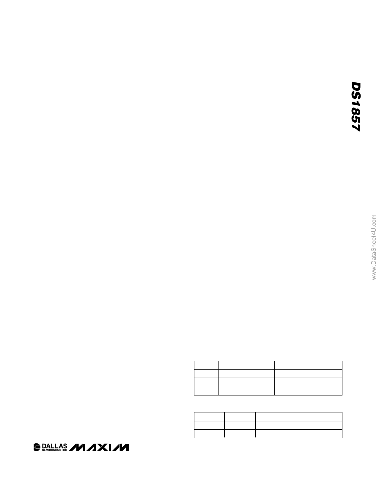
Table 6. Main Device
ADEN configures memory access to respond to differ-
ent device addresses (see Tables 4 and 5).
The default device address for EEPROM-generated
addresses is A2h.
If the ADEN bit is 1, additional 128 bytes of EEPROM
are accessible through the Main Device, selected as
Table 00 (see Figure 3). In this configuration, the
Auxiliary Device address is not accessible. APEN con-
trols the direction of Table 00 regardless of the setting
of ADEN.
WPEN
0
X
1
MPEN
X
0
1
PROTECT MAIN
No
No
Yes
Table 7. Auxiliary Device
APEN
0
1
WPEN
X
X
PROTECT AUXILIARY
No
Yes
____________________________________________________________________ 11
www.DataSheet4U.com
11 Page | ||
| Páginas | Total 22 Páginas | |
| PDF Descargar | [ Datasheet DS1857.PDF ] | |
Hoja de datos destacado
| Número de pieza | Descripción | Fabricantes |
| DS1851 | Dual Temperature-Controlled NV Digital-to-Analog Converters | Dallas Semiconducotr |
| DS1852 | Optical Transceiver Diagnostic Monitor | Dallas Semiconductor |
| DS1854 | Dual Temperature-Controlled Resistors | Maxim Integrated Products |
| DS1855B-010 | Dual Nonvolatile Digital Potentiometer and Secure Memory | Dallas Semiconducotr |
| Número de pieza | Descripción | Fabricantes |
| SLA6805M | High Voltage 3 phase Motor Driver IC. |
Sanken |
| SDC1742 | 12- and 14-Bit Hybrid Synchro / Resolver-to-Digital Converters. |
Analog Devices |
|
DataSheet.es es una pagina web que funciona como un repositorio de manuales o hoja de datos de muchos de los productos más populares, |
| DataSheet.es | 2020 | Privacy Policy | Contacto | Buscar |
