|
|
PDF DAC8555 Data sheet ( Hoja de datos )
| Número de pieza | DAC8555 | |
| Descripción | VOLTAGE OUTPUT DIGITAL-TO-ANALOG CONVERTER | |
| Fabricantes | Burr-Brown Corporation | |
| Logotipo |  |
|
Hay una vista previa y un enlace de descarga de DAC8555 (archivo pdf) en la parte inferior de esta página. Total 27 Páginas | ||
|
No Preview Available !
www.DataSheet4U.com
BurrĆBrown Products
from Texas Instruments
DAC8555 ®
DAC8555
SLAS475A – NOVEMBER 2005 – REVISED DECEMBER 2005
16-BIT, QUAD CHANNEL, ULTRALOW GLITCH, VOLTAGE OUTPUT
DIGITAL-TO-ANALOG CONVERTER
FEATURES
DESCRIPTION
• Relative Accuracy: 12 LSB (Max)
The DAC8555 is a 16-bit, quad channel voltage
• Glitch Energy: 0.15 nV-s
output digital-to-analog converter (DAC) offering
• Power Supply: +2.7 V to +5.5 V
• MicroPower Operation: 850 µA at 5 V
low-power operation and a flexible serial host
interface. It offers monotonicity, good linearity, and
exceptionally low glitch. Each on-chip precision
• 16-Bit Monotonic Over Temperature
output amplifier allows rail-to-rail output swing to be
• Settling Time: 10 µs to ±0.003% FSR
• Power-On Reset to Zero-Scale and Mid-Scale
achieved over the supply range of 2.7 V to 5.5 V. The
device supports a standard 3-wire serial interface
capable of operating with input data clock frequencies
• Binary and 2's Complement Capability
up to 50 MHz for IOVDD = 5 V.
• Ultra-Low AC Crosstalk: –100 dB Typ
The DAC8555 requires an external reference voltage
• On-Chip Output Buffer Amplifier With
to set the output range of each DAC channel. Also
Rail-to-Rail Operation
incorporated into the device is a power-on reset
• Double Buffered Input Architecture
• Simultaneous or Sequential Output Update
and Power-Down
circuit which can be programmed to ensure that the
DAC outputs power up at zero-scale or mid-scale and
remain there until a valid write takes place. The
device also has the capability to function in both
• Asynchronous Clear to Zero-Scale and
binary and 2's complement mode. The DAC8555
Mid-Scale
provides a per channel power-down feature,
• Schmitt-Triggered Inputs
accessed over the serial interface, that reduces the
DataSheet4cUu.crroemnt consumption to 200 nA per channel at 5 V.
• SPI Compatible Serial Interface: Up to 50 MHz.
• 1.8 V to 5.5 V Logic Compatibility
The low-power consumption of this device in normal
operation makes it ideally suited to portable battery-
• Available in a TSSOP-16 Package
operated equipment and other low-power
applications. The power consumption is 5 mW at 5 V,
APPLICATIONS
reducing to 4 µW in power-down mode.
• Portable Instrumentation
• Closed-Loop Servo-Control
• Process Control
The DAC8555 is available in a TSSOP-16 package
with a specified operating temperature range of
–40°C to 105°C.
• Data Acquisition Systems
• Programmable Attenuation
• PC Peripherals
DataShee
Please be aware that an important notice concerning availability, standard warranty, and use in critical applications of Texas
Instruments semiconductor products and disclaimers thereto appears at the end of this data sheet.
SPI, QSPI are trademarks of Motorola.
DataSheet4UM.iccroomwire is a trademark of National Semiconductor.
PRODUCTION DATA information is current as of publication date.
Products conform to specifications per the terms of the Texas
Instruments standard warranty. Production processing does not
necessarily include testing of all parameters.
Copyright © 2005, Texas Instruments Incorporated
1 page 
www.DataSheet4U.com
www.ti.com
PIN NAME
8 VOUTD
9 SYNC
10 SCLK
11 DIN
12 IOVDD
13 RST
14 RSTSEL
15 ENABLE
16 LDAC
DAC8555
SLAS475A – NOVEMBER 2005 – REVISED DECEMBER 2005
PIN DESCRIPTIONS (continued)
DESCRIPTION
Analog output voltage DAC D.
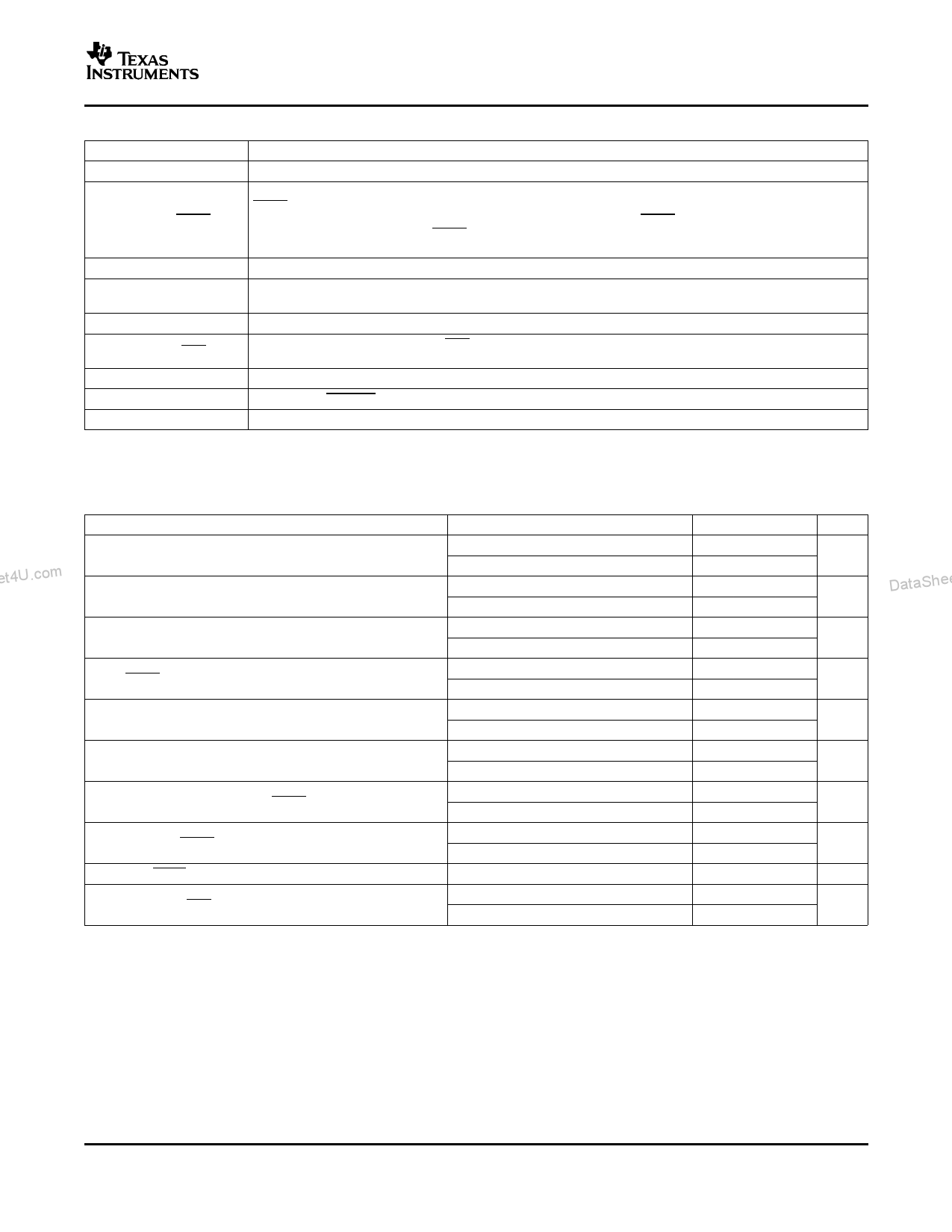
Level-triggered control input (active LOW). This is the frame synchronization signal for the input data. When
SYNC goes LOW, it enables the input shift register and data is transferred in on the falling edges of the
following clocks. The DAC is updated following the 24th clock (unless SYNC is taken HIGH before this edge
in which case the rising edge of SYNC acts as an interrupt and the write sequence is ignored by the
DAC8555).
Serial clock input. Data can be transferred at rates up to 50 MHz.
Serial data input. Data is clocked into the 24-bit input shift register on each falling edge of the serial clock
input.
Digital input-output power supply
Asynchronous reset. Active low. If RST is low, all DAC channels reset either to zero scale (RSTSEL = 0) or to
midscale (RSTSEL = 1).
Reset select. If RSTSEL is low, input coding is binary; if high = 2's complement.
Active LOW, ENABLE LOW connects the SPI interface to the serial port.
Load DACs, rising edge triggered loads all DAC registers.
et4U.com
TIMING REQUIREMENTS(1)(2)
AVDD = 2.7 V to 5.5 V, all specifications –40°C to 105°C (unless otherwise noted)
PARAMETER
TEST CONDITIONS
t
(3)
1
t2
t3
t4
t5
t6
t7
t8
t9
t 10
SCLK cycle time
IOVDD = AVDD = 2.7 V to 3.6 V
IOVDD = AVDD = 3.6 V to 5.5 V
SCLK HIGH time
SCLK LOW time
IOVDD = AVDD = 2.7 V to 3.6 V
DataSIOheVeDDt4=UA.VcDoDm= 3.6 V to 5.5 V
IOVDD = AVDD = 2.7 V to 3.6 V
IOVDD = AVDD = 3.6 V to 5.5 V
SYNC falling edge to SCLK rising edge setup time
IOVDD = AVDD = 2.7 V to 3.6 V
IOVDD = AVDD = 3.6 V to 5.5 V
Data setup time
IOVDD = AVDD = 2.7 V to 3.6 V
IOVDD = AVDD = 3.6 V to 5.5 V
Data hold time
IOVDD = AVDD = 2.7 V to 3.6 V
IOVDD = AVDD = 3.6 V to 5.5 V
24th SCLK falling edge to SYNC rising edge
IOVDD = AVDD = 2.7 V to 3.6 V
IOVDD = AVDD = 3.6 V to 5.5 V
Minimum SYNC HIGH time
IOVDD = AVDD = 2.7 V to 3.6 V
IOVDD = AVDD = 3.6 V to 5.5 V
24th SCLK falling edge to SYNC falling edge
IOVDD = AVDD = 2.7 V to 5.5 V
Miniumum RST low time
IOVDD = AVDD = 2.7 V to 3.5 V
IOVDD = AVDD = 3.6 V to 5.5 V
MIN TYP MAX UNIT
40
ns
20
20
ns
10
20
ns
10
0
ns
0
5
ns
5
4.5
ns
4.5
0
ns
0
40
ns
20
130 ns
40
ns
20
(1) All input signals are specified with tR = tF = 3 ns (10% to 90% of AVDD) and timed from a voltage level of (VIL + VIH)/2.
(2) See Serial Write Operation timing diagram.
(3) Maximum SCLK frequency is 50 MHz at IOVDD = AVDD = 3.6 V to 5.5 V and 25 MHz at IOVDD = AVDD = 2.7 V to 3.6 V.
DataShee
DataSheet4U.com
5
5 Page 
www.DataSheet4U.com
DAC8555
www.ti.com
SLAS475A – NOVEMBER 2005 – REVISED DECEMBER 2005
TYPICAL CHARACTERISTICS (continued)
At TA = 25°C, unless otherwise noted
FULL-SCALE SETTLING TIME: 5 V RISING EDGE
FULL-SCALE SETTLING TIME: 5 V FALLING EDGE
Trigger Pulse
5 V/div
Trigger Pulse
5 V/div
AVDD = 5 V,
Vref = 4.096 V,
From Code: 0000
To Code: FFFF
AVDD = 5 V,
Vref = 4.096 V,
From Code: FFFF
To Code: 0000
Rising
Edge
1 V/div
Zoomed Rising Edge
1 mV/div
Time (2 µs/div)
Figure 25.
HALF-SCALE SETTLING TIME: 5 V RISING EDGE
Falling
Edge
1 V/div
Zoomed Falling Edge
1 mV/div
Time (2 µs/div)
Figure 26.
HALF-SCALE SETTLING TIME: 5 V FALLING EDGE
et4U.com
Rising
Edge
1 V/div
Trigger Pulse
5 V/div
Falling
Edge
1 V/div
AVDD = 5 V,
Vref = 4.096 V,
DataSheet4U.com
From Code: 4000
To Code: CFFF
Zoomed Rising Edge
1 mV/div
Trigger Pulse
5 V/div
AVDD = 5 V,
Vref = 4.096 V,
From Code: CFFF
To Code: 4000
Zoomed Falling Edge
1 mV/div
Time (2 µs/div)
Figure 27.
FULL-SCALE SETTLING TIME: 2.7 V RISING EDGE
Time (2 µs/div)
Figure 28.
FULL-SCALE SETTLING TIME: 2.7 V FALLING EDGE
DataShee
Rising
Edge
0.5 V/div
Trigger Pulse
2.7 V/div
AVDD = 2.7 V,
Vref = 2.5 V,
From Code: 0000
To Code: FFFF
Zoomed Rising Edge
1 mV/div
Time (2 µs/div)
Figure 29.
Falling
Edge
0.5 V/div
Trigger Pulse
2.7 V/div
AVDD = 2.7 V,
Vref = 2.5 V,
From Code: FFFF
To Code: 0000
Zoomed Falling Edge
1 mV/div
Time (2 µs/div)
Figure 30.
DataSheet4U.com
11
11 Page | ||
| Páginas | Total 27 Páginas | |
| PDF Descargar | [ Datasheet DAC8555.PDF ] | |
Hoja de datos destacado
| Número de pieza | Descripción | Fabricantes |
| DAC8550 | VOLTAGE OUTPUT DIGITAL-TO-ANALOG CONVERTER | Burr-Brown Corporation |
| DAC8550 | DAC8550 16-bit Ultra-Low Glitch Voltage Output Digital-To-Analog Converter (Rev. F) | Texas Instruments |
| DAC8551 | VOLTAGE OUTPUT DIGITAL-TO-ANALOG CONVERTER | Burr-Brown Corporation |
| DAC8551 | DAC8551 16-Bit Ultralow-Glitch Voltage-Output Digital to Analog Converter (Rev. C) | Texas Instruments |
| Número de pieza | Descripción | Fabricantes |
| SLA6805M | High Voltage 3 phase Motor Driver IC. |
Sanken |
| SDC1742 | 12- and 14-Bit Hybrid Synchro / Resolver-to-Digital Converters. |
Analog Devices |
|
DataSheet.es es una pagina web que funciona como un repositorio de manuales o hoja de datos de muchos de los productos más populares, |
| DataSheet.es | 2020 | Privacy Policy | Contacto | Buscar |
